Semiconductor device

A technology for semiconductors and devices, applied in the field of semiconductor devices, can solve the problems of reducing the area of ​​integrated circuits, difficulty in circuit scale, and restrictions on the use of ID chips, and achieve the effects of reducing connection failures, enhancing gain, and easing size constraints

Inactive Publication Date: 2007-03-28
SEMICON ENERGY LAB CO LTD
View PDF0 Cites 7 Cited by
  • Summary
  • Abstract
  • Description
  • Claims
  • Application Information

AI Technical Summary

Problems solved by technology

However, this case is not favorable because securing the circuit scale is difficult and the use of ID chips is limited
Therefore, it is disadvantageous that the area of ​​the integrated circuit is reduced when securing the circuit scale of the integrated circuit without careful consideration

Method used


Image

  • Semiconductor device
  • Semiconductor device
  • Semiconductor device

Examples


Embodiment 1

[0102] A specific method for manufacturing the ID chip of the present invention will be described. In this embodiment, a TFT is given as an example of a semiconductor element. However, semiconductor elements used in integrated circuits are not limited thereto, and various circuit elements may be used.

[0103] As shown in FIG. 10A , a separation layer 501 is formed over a heat-resistant first substrate 500 . For example, a glass substrate such as barium borosilicate glass or aluminoborosilicate glass, a quartz substrate, a ceramic substrate, etc. may be used for the first substrate 500 . In addition, a metal substrate including a SUS substrate or a semiconductor substrate may be used. Substrates made of a flexible synthetic resin such as plastic generally tend to be less resistant to high temperatures than the substrates described above. However, such a substrate made of synthetic resin can be used as long as it can withstand the processing temperature in the manufacturing ...

Embodiment 2

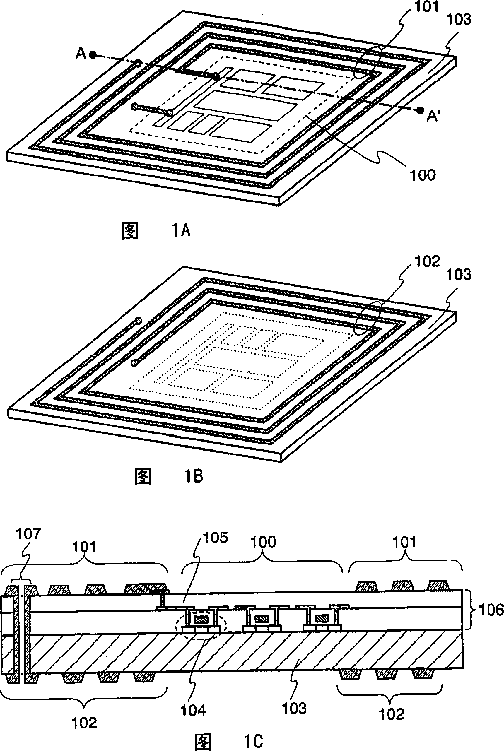
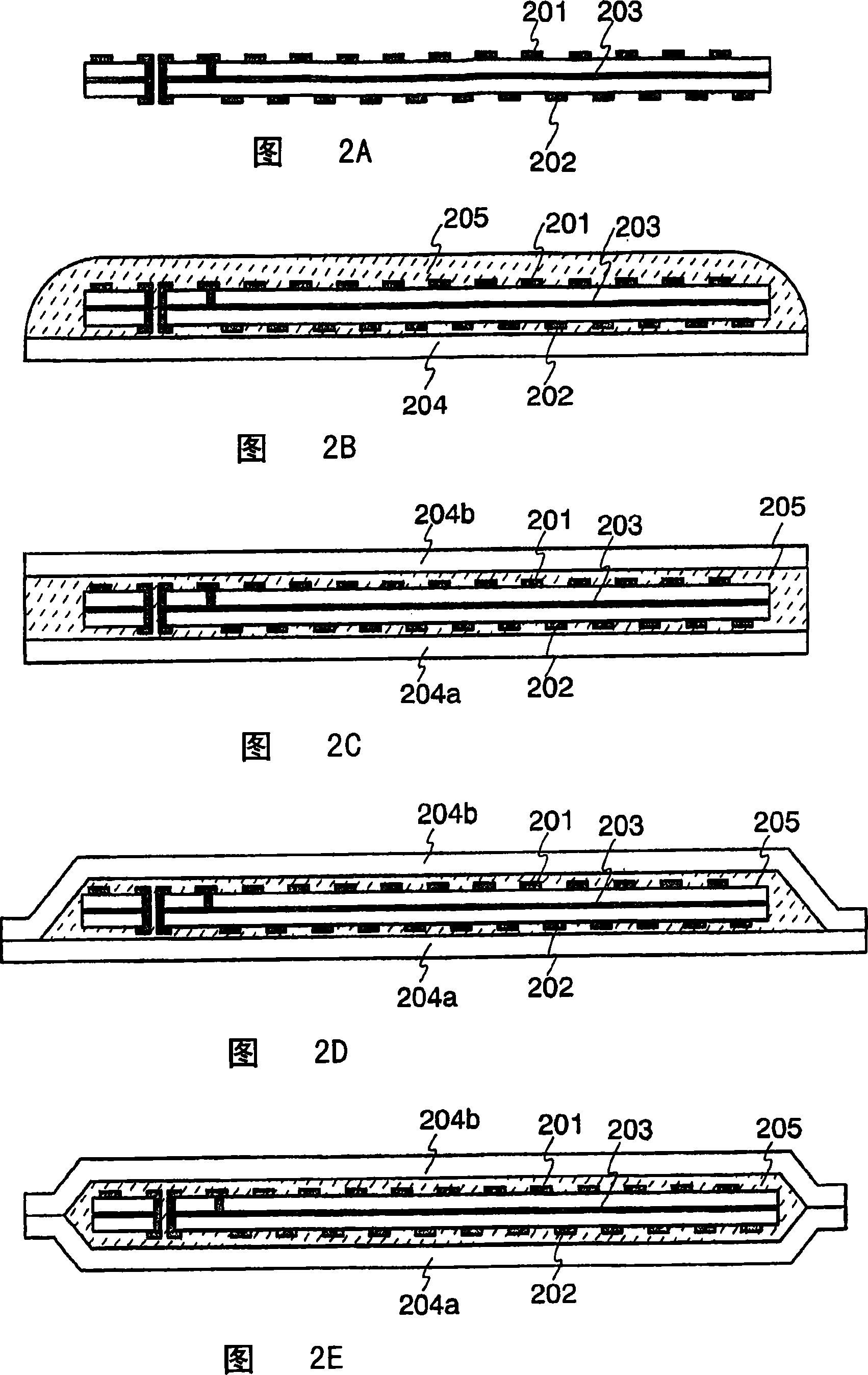
[0174] In this embodiment, a method for manufacturing a plurality of ID chips using a large substrate will be described.

[0175] A plurality of integrated circuits 401 are formed over a substrate 400 . Thereafter, a contact hole 403 for connecting a first wire 404 and a second wire 405 to be formed later is formed. FIG. 16A shows a state where a plurality of integrated circuits 401 corresponding to each ID chip are formed over a substrate 400 . FIG. 16B shows an enlarged view of the area surrounded by the dashed line 402 of FIG. 16A.

[0176] Next, a first wire 404 is formed on the side where the integrated circuit 401 is formed, and a second wire is formed on the side opposite to the side where the integrated circuit 401 is formed. FIG. 16C shows an enlarged view of the area surrounded by the dashed line 402 in FIG. 16A after the first wire 404 is formed. As shown in FIG. 16C , the first wire 404 is formed to overlap the contact hole 403 . Accordingly, the first wire 404...

Embodiment 3

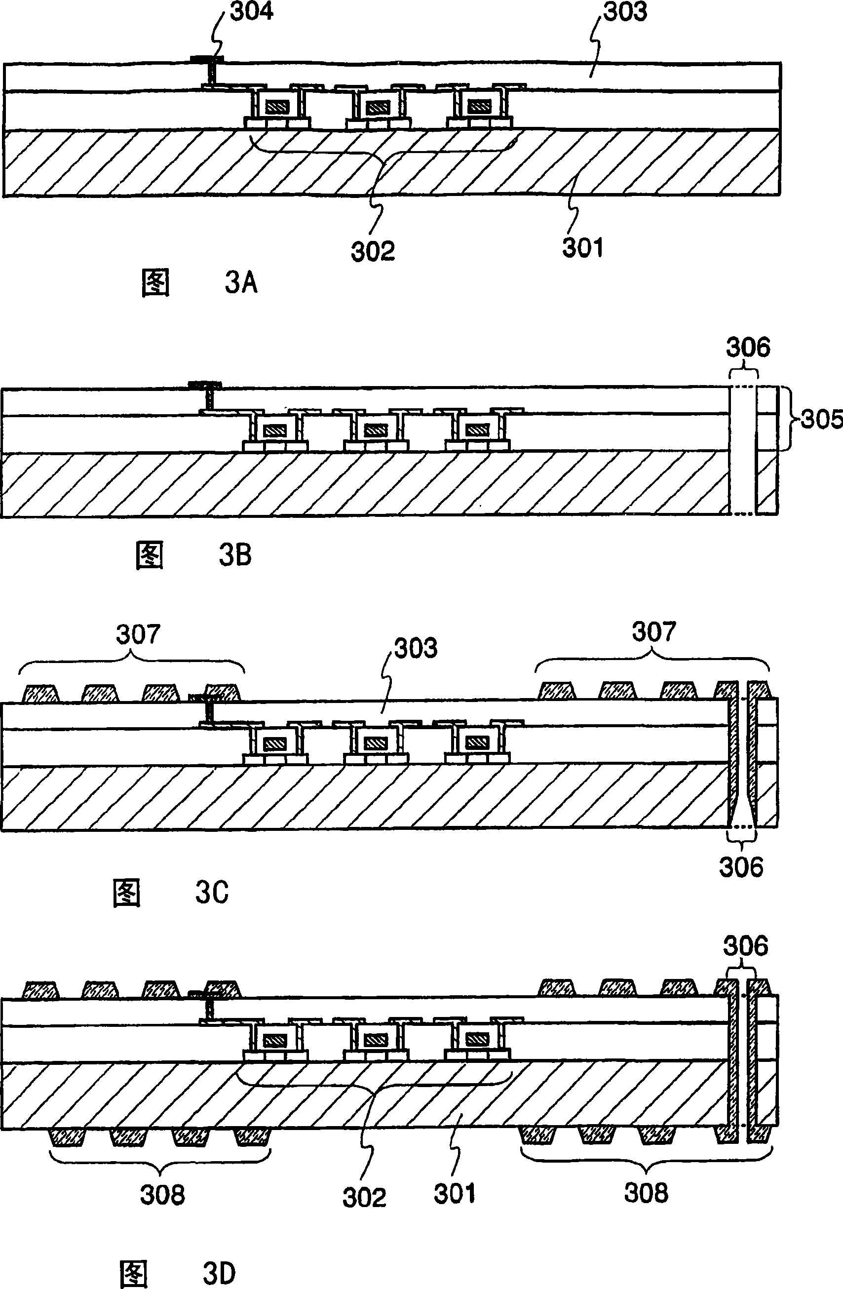
[0181] In this embodiment, the structure of a TFT used in the ID chip of the present invention will be described.

[0182] FIG. 17A shows a cross-sectional view of a TFT according to this embodiment. Reference numeral 701 denotes an n-channel TFT; 702, a p-channel TFT. The structure of the n-channel TFT 701 will be described in detail as an example.

[0183] An n-channel TFT 701 includes an island-shaped semiconductor film 705 serving as an active layer. The island-shaped semiconductor film 705 includes two impurity regions 703 serving as source and drain regions, a channel formation region 704 sandwiched between the two impurity regions 703, and a channel formation region 704 sandwiched between the impurity regions 703 and the channel formation region 704. Two LDD (Lightly Doped Drain) regions 710. The n-channel TFT 701 further includes a gate insulating film 706 covering the island-shaped semiconductor film 705, a gate electrode 707, and two side walls 708 and 709 made of...


PUM


Abstract

It is an object of the present invention to provide an ID chip in which gain of an antenna is increased and the mechanical strength of an integrated circuit can be enhanced without suppressing a circuit scale. A semiconductor device typified by an ID chip of the present invention includes an integrated circuit using a semiconductor element formed from a thin semiconductor film and an antenna connected to the integrated circuit. The antenna and the integrated circuit are formed on a substrate, and a conducting wire or a conductive film included in the antenna is divided into two layers and formed so as to sandwich the substrate provided with the integrated circuit.

Description

technical field [0001] The present invention relates to a semiconductor device capable of wireless communication. Background technique [0002] Semiconductor devices such as ID chips that can transmit and receive data such as wireless identification information have come into practical use in various fields, and the market for such semiconductor devices as a new mode of communication information terminals is expected to further develop. The ID chip is also called a wireless tag, an RFID (Radio Frequency Identification) tag, or an IC tag, and a type having an integrated circuit formed using a semiconductor substrate and an antenna is now being put into practical use. [0003] There are two cases of forming the ID chip, one is to subsequently connect the separately formed integrated circuit and antenna, and the other is to form the integrated circuit and the antenna so as to be distributed on one substrate. [0004] For an ID chip formed by connecting an integrated circuit an...

Claims


Application Information

Patent Timeline
Patent Type & Authority Applications(China)
IPC IPC(8): H01Q1/38B42D15/10G06K19/077H01Q1/24H01Q7/00H01L21/77H01L27/13
CPCG06K19/07728H01L27/13G06K19/07749H01L2225/06513H01L2225/06541H01L27/1266H01L2224/16145G06K19/07784G06K19/07779H01L2223/6677G06K19/07783H01L27/1214G06K19/077H01Q1/24
Inventor 山崎舜平秋叶麻衣
Owner SEMICON ENERGY LAB CO LTD
Why Eureka
Try Eureka