Method for producing active matrix organic LED panel

A technology of light-emitting diodes and manufacturing methods, which is applied in semiconductor/solid-state device manufacturing, electrical components, circuits, etc., can solve the problems of reduced production capacity and yield, cumbersome steps, complicated processes, etc., and achieve the effect of reducing costs and simplifying processes

Inactive Publication Date: 2007-04-11
CHUNGHWA PICTURE TUBES LTD
View PDF0 Cites 12 Cited by
  • Summary
  • Abstract
  • Description
  • Claims
  • Application Information

AI Technical Summary

Problems solved by technology

[0006] In the prior art, it is necessary to use seven photomasks to complete the fabrication of the organic light-emitting diode panel applied to the thin film transistor array. Not only the steps are cumbersome and the process is complicated, but also the high cost and alignment error caused by the number of photomasks ( misalignment), also seriously reduce production capacity and yield

Method used


Image

  • Method for producing active matrix organic LED panel
  • Method for producing active matrix organic LED panel
  • Method for producing active matrix organic LED panel

Examples


Embodiment Construction

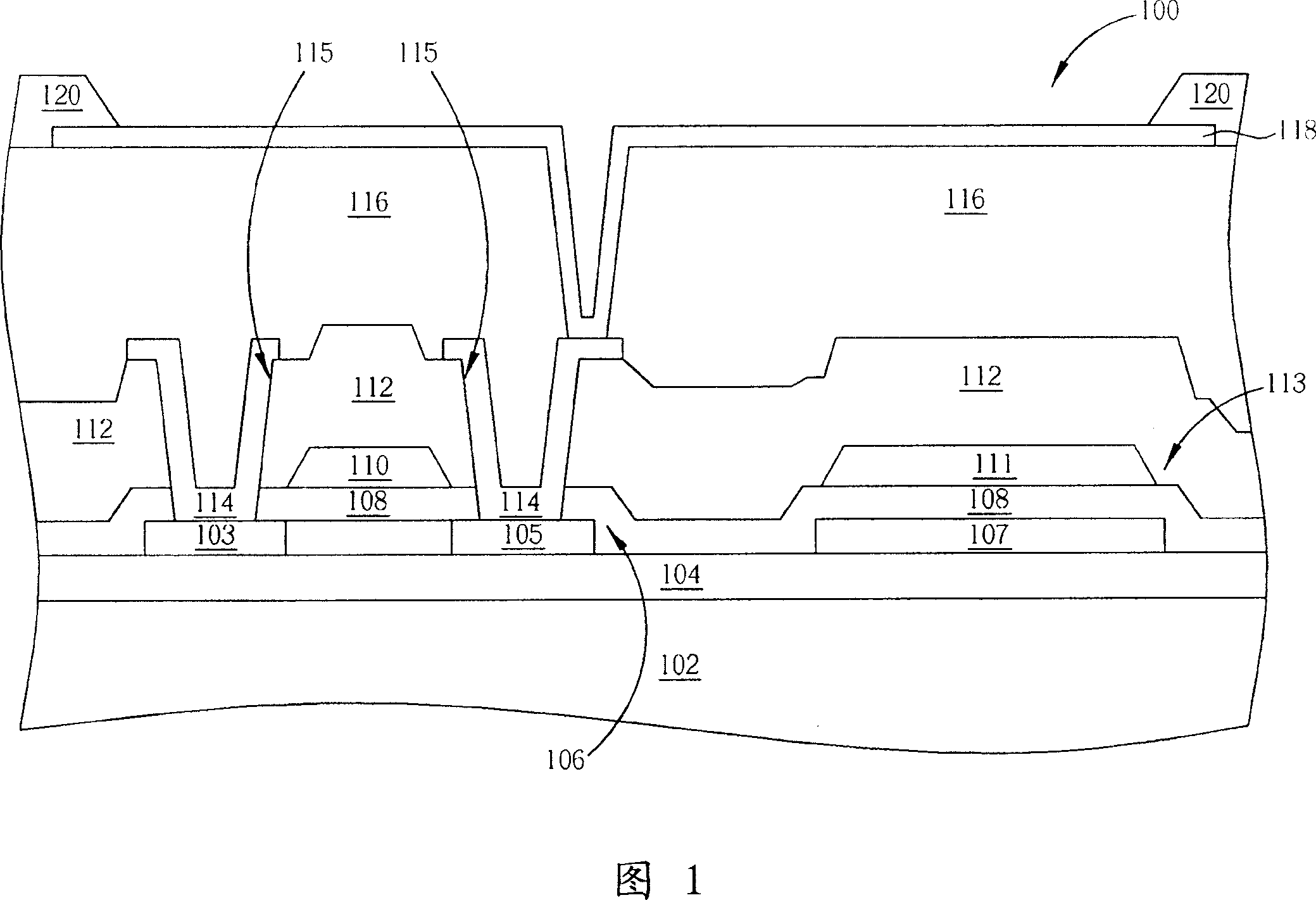
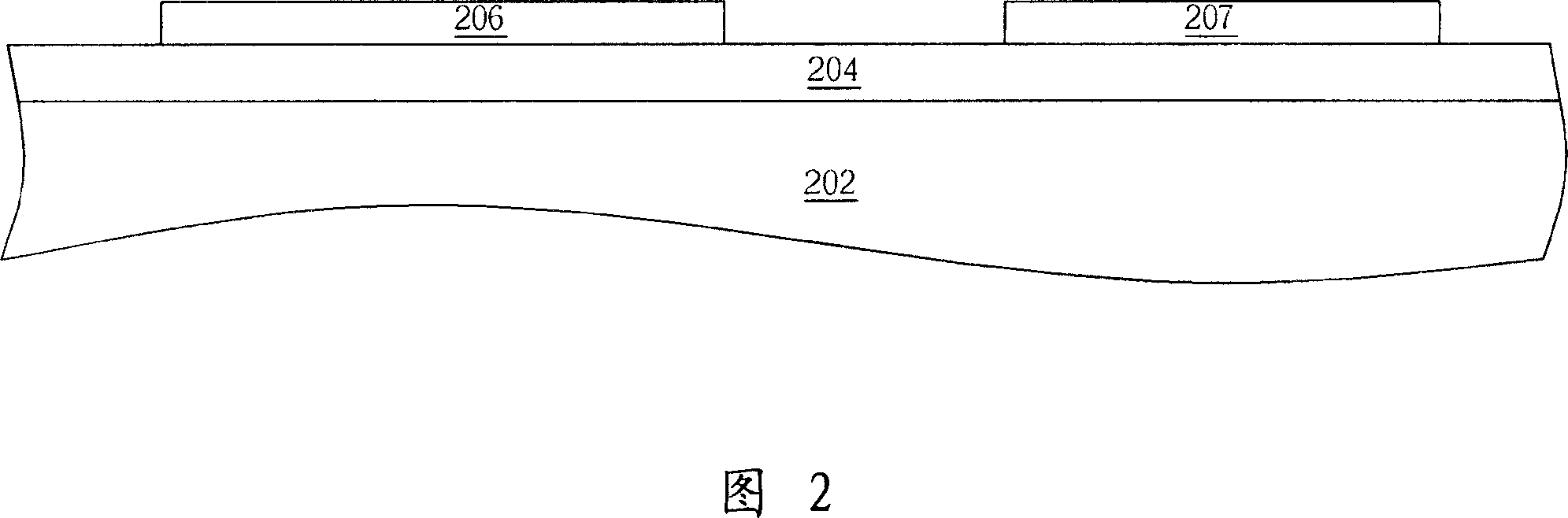
[0032] Please refer to FIG. 2 to FIG. 6 . FIG. 2 to FIG. 6 are process schematic diagrams of the active matrix organic light emitting diode panel (AMOLED) of the present invention. As shown in FIG. 2 , first a glass substrate 202 is provided as the lower substrate, and then a layer of buffer insulating layer 204 and a layer of amorphous silicon thin film (not shown) are sequentially deposited on the glass substrate 202, and then excimer laser etc. An annealing process recrystallizes the amorphous silicon film (not shown) into a polysilicon film. Then, a first photolithography process is performed using a first photomask to etch the desired pattern of the active layer 206 out of the polysilicon film. Wherein, the present invention can also use the above-mentioned first photolithography process to form a polysilicon lower electrode plate 207 in each pixel region according to the needs of the circuit design.

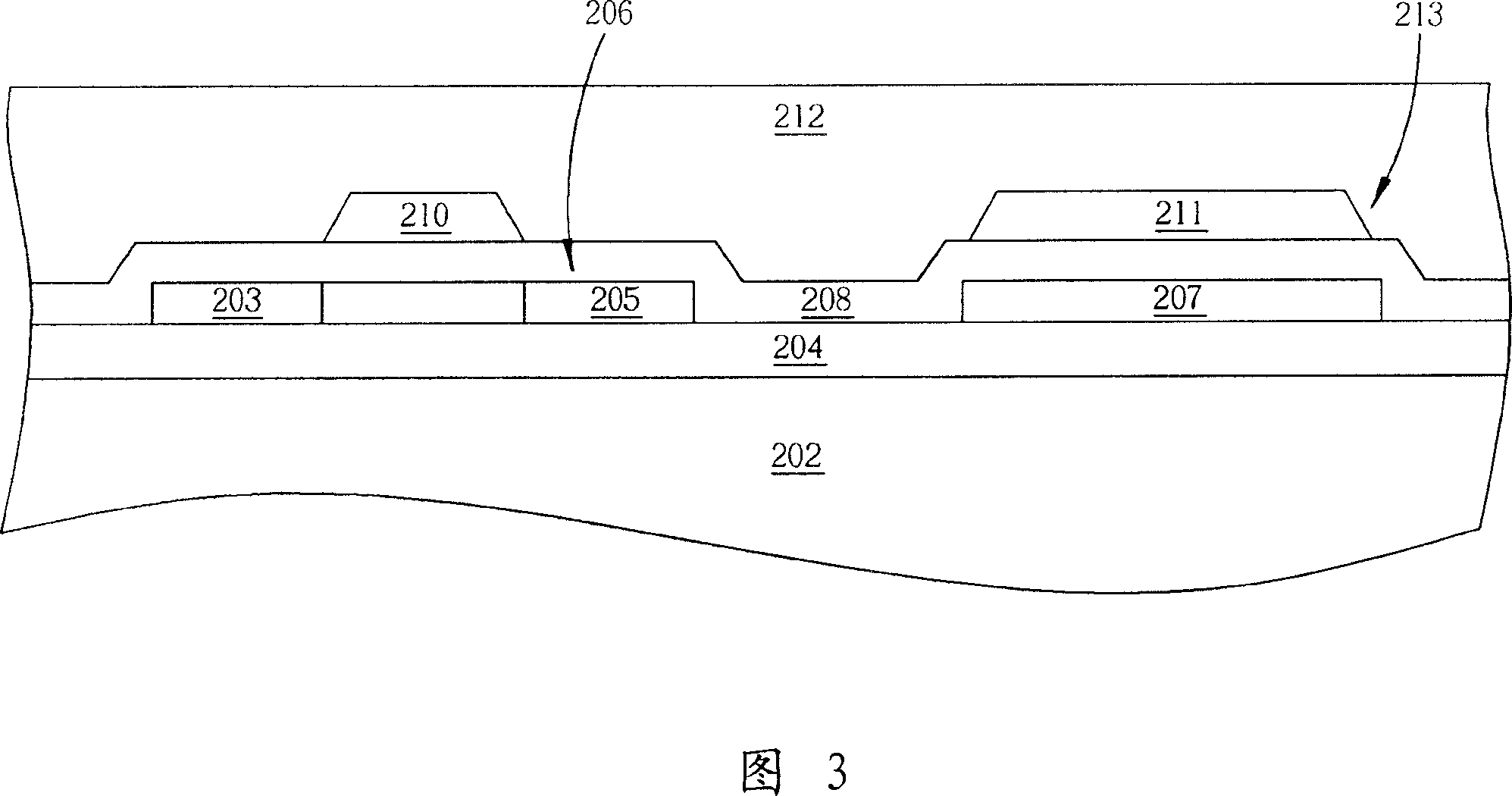
[0033] Referring to FIG. 3 , a gate insulating layer 208 is subsequen...


PUM


Abstract

This invention provides a manufacturing method for an organic LED panel of an active matrix including: providing a base plate, forming a film transistor on the base plate, forming an interlaminar insulation layer to cover the transistor and the base plate, forming multiple through holes to the surfaces of the source and drain of the transistor, forming metal layers in the through holes to be connected with the source and drain, forming transparent electrodes on the surfaces of the metal layers connected to the drain, forming pixel electrode insulation layers to the transparent electrode and the interlaminar insulation layer and forming a LED on the transparent electrode.

Description

technical field [0001] The invention relates to a method for manufacturing a flat panel display, in particular to a method for manufacturing an organic light-emitting diode panel with a low-temperature polysilicon thin film transistor. Background technique [0002] Generally, the steps of manufacturing low temperature polycrystalline silicon thin film transistor (LTPS TFT) arrays need to use as many as six to nine photomasks for photo-etching-process, which is far more than that of ordinary amorphous silicon thin film Five photomasks for a hydrogenated amorphous silicon thin film transistor (α-Si:H TFT) are complex and time-consuming. In addition, in the application of active matrix organic light-emitting diode (AMOLED) panel, due to the complex pixel circuit design structure, it must be manufactured by using low-temperature polysilicon thin film transistor drive array, but because of the many An insulating layer (pixel define layer, PDL) defining the light-emitting area of...

Claims


Application Information

Patent Timeline
Patent Type & Authority Applications(China)
IPC IPC(8): H01L21/84H01L21/82
Inventor 陈振铭
Owner CHUNGHWA PICTURE TUBES LTD
Why Eureka
Try Eureka