Solid-state imaging device, optical sensor, and solid-state imaging device operation method

A solid-state imaging device and pixel technology, which can be used in radiation control devices, image communication, color TV components, etc., can solve problems such as low sensitivity, high sensitivity and wide dynamic range, and inability to match two images

Active Publication Date: 2007-05-16
TOHOKU UNIV
View PDF4 Cites 28 Cited by
  • Summary
  • Abstract
  • Description
  • Claims
  • Application Information

AI Technical Summary

Problems solved by technology

[0014] However, in the methods described in Patent Documents 1, 2, and 3 and Non-Patent Document 2 or in the method of capturing images twice with different exposure times, it is necessary to perform the imaging on the low-illuminance side and the one on the high-illuminance side at different timings. side camera, so if a moving image is captured, there will be a shift in the captured image corresponding to the two illuminances, and there is a problem that the two images cannot be matched.
[0015] In addition, in the methods described in Patent Document 4 and Non-Patent Document 3, a wide dynamic range can be realized for imaging on the high-illuminance side, but low sensitivity, low S / N ratio, cannot improve image quality
[0016] As mentioned above, in image sensors such as CMOS image sensors, it is difficult to achieve a wide dynamic range while maintaining high sensitivity and high S / N ratio
[0017] In addition, this fact is not limited to image sensors, and it is also difficult to achieve a wide dynamic range while maintaining high sensitivity and a high S / N ratio as a line sensor in which pixels are arranged in a straight line or a photosensor that does not have many pixels.

Method used


Image

  • Solid-state imaging device, optical sensor, and solid-state imaging device operation method
  • Solid-state imaging device, optical sensor, and solid-state imaging device operation method
  • Solid-state imaging device, optical sensor, and solid-state imaging device operation method

Examples


Embodiment 1

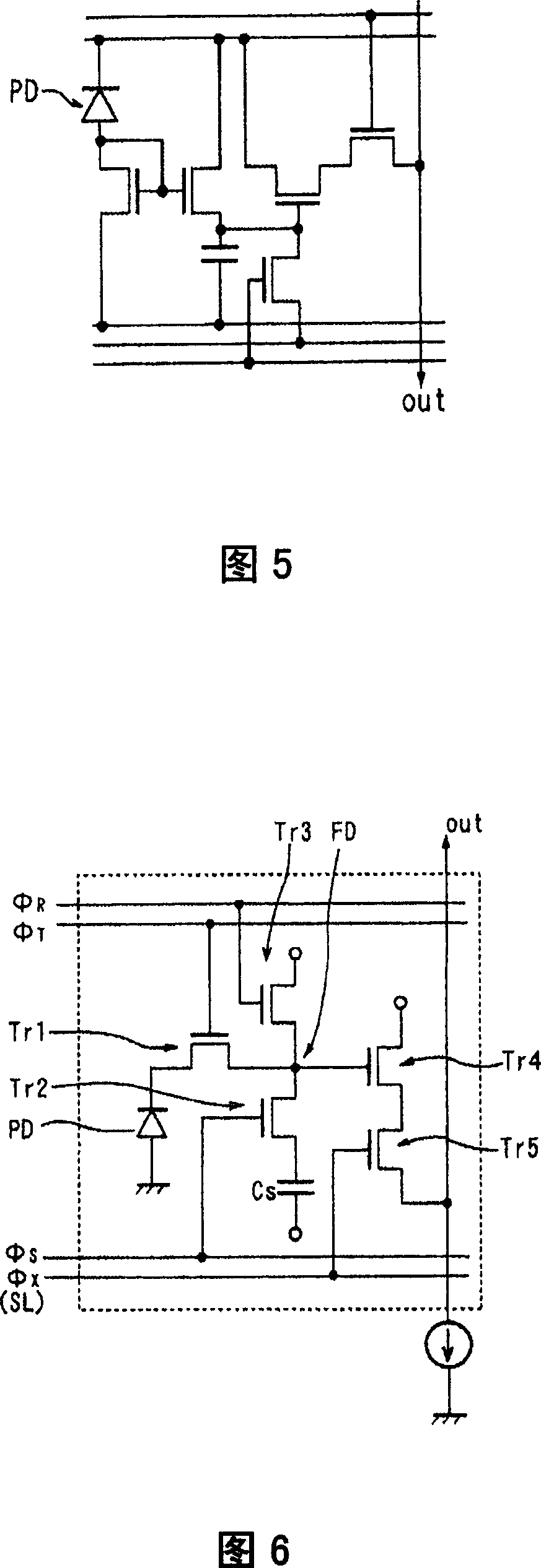
[0105] The solid-state imaging device of this embodiment is a CMOS image sensor, and FIG. 6 is an equivalent circuit diagram of one pixel.

[0106] Each pixel consists of a photodiode PD that receives light and generates and accumulates photocharges, a transfer transistor Tr1 that transfers photocharges from the photodiode PD, and a floating diffusion FD that transfers photocharges through the transfer transistor. Said photodiode overflows the photocharge accumulation capacitor element C S , The floating diffusion FD and the storage capacitor element C S The storage transistor Tr2 that is combined or divided by the potential of the floating diffusion FD is connected to the reset transistor Tr3 that is formed on the floating diffusion FD and used to discharge the photocharge in the floating diffusion FD, and amplifies and converts the photocharge in the floating diffusion FD into a voltage signal. The amplifying transistor Tr4 and the selection transistor Tr5 connected to the ...

Embodiment 2

[0192] The CMOS image sensor of this embodiment is the same as the CMOS image sensor of Embodiment 1, but the driving method is different.

[0193] Figure 16 shows the drive line (Φ T 、Φ S 、Φ R ) Timing diagram of the voltage applied across . Like Embodiment 1, it can be about Φ T Add the 3 levels of the energy level represented by (+α).

[0194] First, at time T when a new picture starts 0 , at Φ T is off, Φ S In the state of on, Φ R When it is on, the photocharge generated in the previous screen is completely discharged and reset.

[0195] for C PD The savings period T PD from time T 0 Previous Φ T start at the moment of off, in C PD The accumulation of photoelectric charge starts.

[0196] Then, at time T 0 The moment after the reset of T 1 , Φ R is off. At this time, become C FD and C S combined state, put the C FD +C S signal of the reset level as noise N 2 Read and store in the frame memory. At supersaturation, the noise N 2 is very small, so ins...

Embodiment 3

[0232] The CMOS image sensor of embodiment 1 and 2, or in embodiment 1 from moment T 0 Storage capacitor storage period T CS To start the mode of CMOS image sensor, put C FD +C S signal of the reset level as noise N 2 Read out and store in the frame memory FM, thereby canceling the sum of the charge signal before saturation and the oversaturated charge signal (S 1 +S 2 ) noise during sampling, but in the CMOS image sensor of this embodiment, no frame memory is used, which can reduce chip cost.

[0233] C FD +C S signal of the reset level (N2 ) The sampling timing ratio of the modulated pre-saturation charge signal and the sum of the oversaturation charge signal (S 1 ’+S 2 ’+N 2 ) sampling timing occurs earlier by 1 frame, so a frame memory is necessary.

[0234] Here, C FD +C S signal of the reset level (N 2 ) by C FD signal of the reset level (N 1 ) or N of the next frame 2 (expressed as N 2 ”) substitution, which cancels out the threshold bias of the in-pixe...


PUM


Abstract

There are provided a solid-sate imaging device and an optical sensor which can have a wide dynamic range while maintaining a high sensitivity and a high S/N ratio, and a solid-state device operation method for having a wide dynamic range while maintaining the high sensitivity and the high S/N ratio. Each of the pixels has a photodiode PD for receiving light and generating and accumulating photoelectric charge and an accumulation capacity element Cs for accumulating photoelectric charge flowing out from the photodiode which are connected via a transfer transistor Tr1. The pixels are accumulated in an array shape. Here, the accumulation capacity element Cs has a configuration for accumulating photoelectric charge flowing out from the photodiode PD in the accumulation capacity element accumulation period Tcs set with a predetermined period ratio from the accumulation period of the photodiode PD.

Description

technical field [0001] The present invention relates to a solid-state imaging device, an optical sensor, and an operating method of the solid-state imaging device, and more particularly, to a CMOS-type solid-state imaging device, an optical sensor, and an operating method of the solid-state imaging device. Background technique [0002] Image input image sensors such as CMOS (Complementary Metal-Oxide-Semiconductor) image sensors and CCD (Charge Coupled Device) image sensors need to be widely used in digital cameras and mobile phones with cameras as their characteristics improve. [0003] The image sensor is expected to further improve its characteristics, one of which is to expand the dynamic range. [0004] The dynamic range of image sensors used in the past is, for example, around 3 to 4 digits (60 to 80 dB), but currently it cannot reach the 5 to 6 digits (100 to 120 dB) of the naked eye or silver salt thin film. [0005] Therefore, it is desired to develop a high image ...

Claims


Application Information

Patent Timeline
Patent Type & Authority Applications(China)
IPC IPC(8): H04N5/335H01L27/146
Inventor 须川成利足立理矢幡恭一寺田达矢
Owner TOHOKU UNIV
Why Eureka
Try Eureka