Optical modulating circuit and optical modulating method
一种光调制、电路的技术,应用在光多路复用系统、光学、电气元件等方向,能够解决数据率频带限制等问题
- Summary
- Abstract
- Description
- Claims
- Application Information
AI Technical Summary
Problems solved by technology
Method used
Image

Examples
no. 1 Embodiment approach
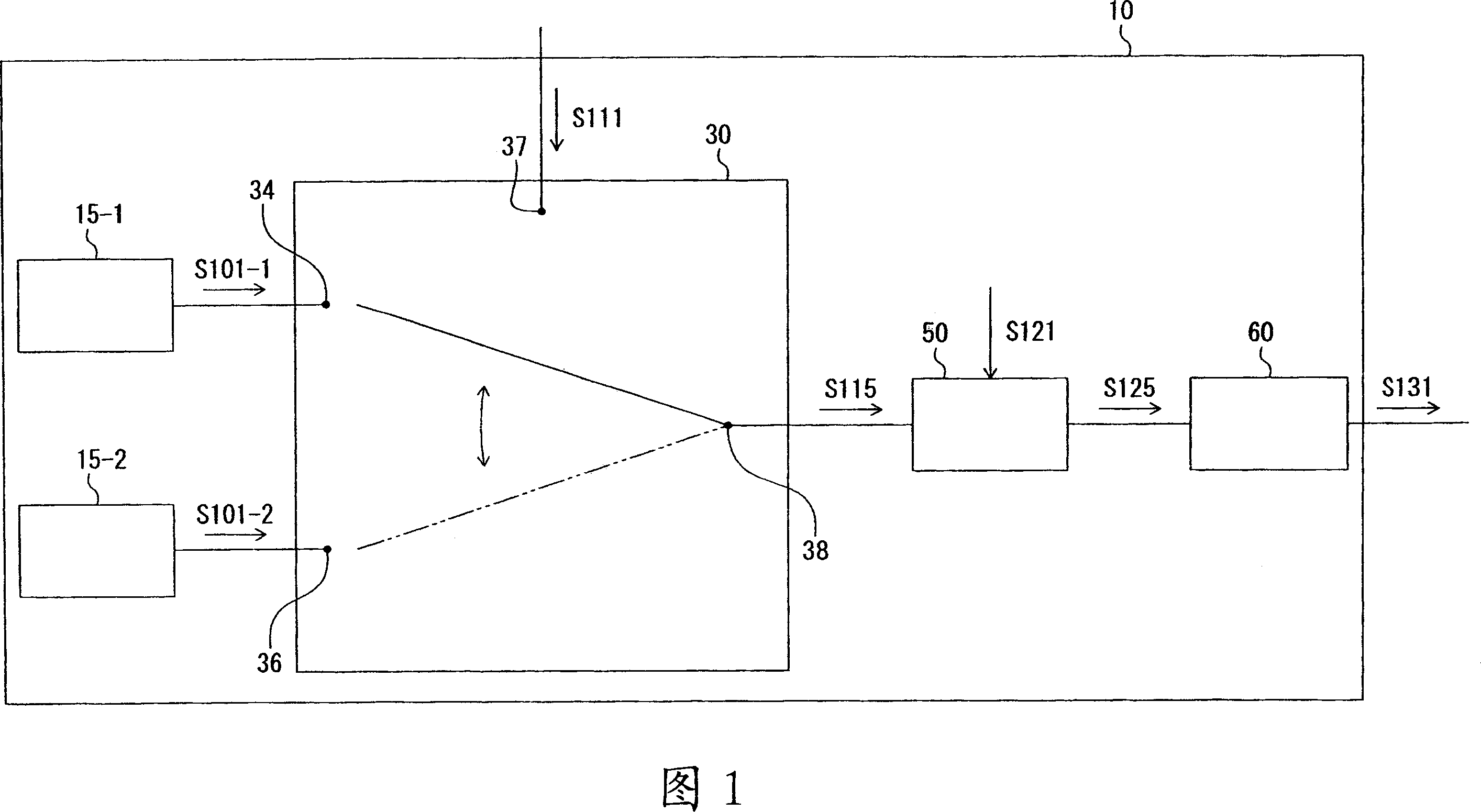
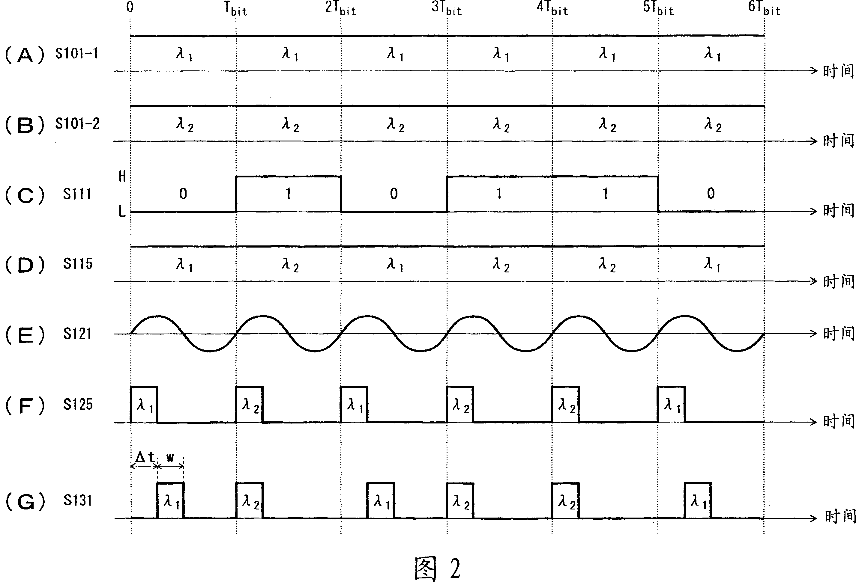
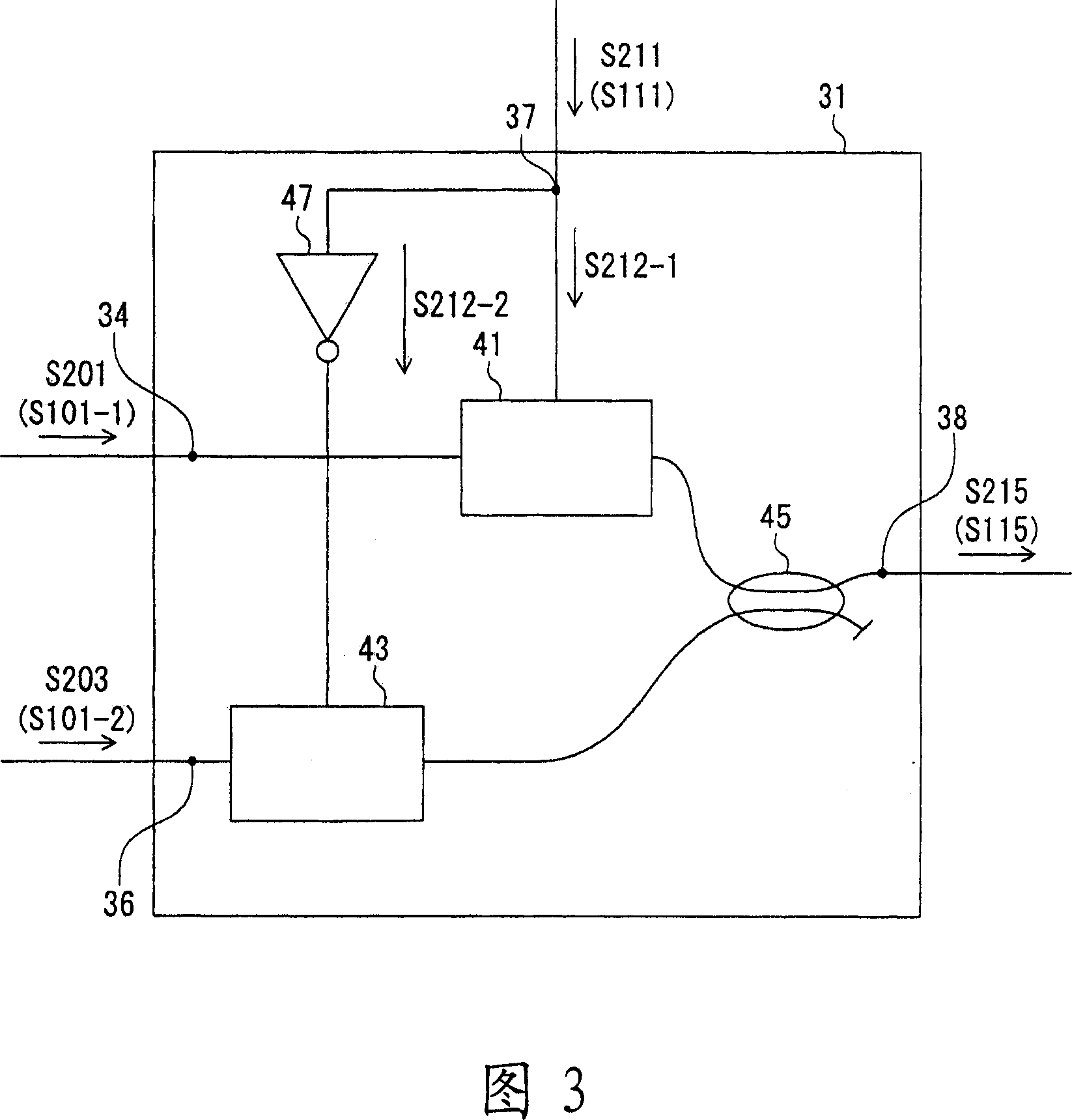
[0066] An optical modulation circuit and an optical modulation method according to a first embodiment will be described with reference to FIGS. 1 and 2 . FIG. 1 is a schematic configuration diagram illustrating an optical modulation circuit according to a first embodiment. FIG. 2 is a timing chart for explaining the operating principle of the optical modulation circuit. In FIG. 2, the horizontal axis represents time. In addition, on the vertical axis, the magnitude of each signal is represented by voltage for electrical signals, and light intensity for optical signals. In Figure 2, the reference position on the time axis is equal to the data period T bit time interval, from 0, T bit , 2T bit 、3T bit 、4T bit , 5T bit and 6T bit express.
[0067] The optical modulation circuit 10 is configured to include a first light source 15 - 1 , a second light source 15 - 2 , an optical switch 30 , an optical modulator 50 , and a delay unit 60 .
[0068] The first light source 15 ...
no. 2 Embodiment approach
[0113] An optical modulation circuit and an optical modulation method according to the second embodiment will be described with reference to FIGS. 6 and 7 . FIG. 6 is a schematic configuration diagram illustrating an optical modulation circuit according to a second embodiment. FIG. 7 is a timing chart for explaining the operating principle of the optical modulation circuit. In FIG. 7, the horizontal axis represents time. Also, the vertical axis represents the magnitude of each signal, and electrical signals are represented by voltage, while optical signals are represented by light intensity.
[0114] In the optical modulation circuit and the optical modulation method of the second embodiment, in one data cycle T 2bits The modulation method used in the case of transmitting 2-bit information within 4(=2 2 ) value pulse position modulation.
[0115] The optical modulation circuit 11 is configured to include first to fourth light sources 15 - 1 to 4 , an optical switch unit 70...
no. 3 Embodiment approach
[0142] An optical modulation circuit and an optical modulation method according to a third embodiment will be described with reference to FIG. 10 . FIG. 10 is a schematic configuration diagram for explaining an optical modulation circuit according to a third embodiment.
[0143] In the optical modulation circuit and optical modulation method of the third embodiment, one data period T nbits The modulation method used in the case of transmitting n-bit information within a 2 n Pulse position modulation of the value.
[0144] The optical modulation circuit 12 is configured to include: first to second n Light source 15-1~2 n , the optical switch unit 170 , the optical modulator 50 and the delay unit 161 . In addition, since the optical modulator 50 may have the same configuration as that described in the first embodiment, description thereof will be omitted here.
[0145] 1st to 2nd n Light source 15-1~2 n For example, it is composed of any appropriate conventionally known s...
PUM
 Abstract
Description
Claims
Application Information
 - R&D
- Intellectual Property
- Life Sciences
- Materials
- Tech Scout
- Unparalleled Data Quality
- Higher Quality Content
- 60% Fewer Hallucinations
Browse by: Latest US Patents, China's latest patents, Technical Efficacy Thesaurus, Application Domain, Technology Topic, Popular Technical Reports.
© 2025 PatSnap. All rights reserved.Legal|Privacy policy|Modern Slavery Act Transparency Statement|Sitemap|About US| Contact US: help@patsnap.com