Anisotropic conductive connector for wafer inspection, production method and application therefor

An anisotropic, manufacturing method technology, applied in the direction of conductive connection, electrical component connection, elastic body connector, etc., can solve the problems of complicated manufacturing process, high manufacturing cost of anisotropic conductive connector, and increased wafer inspection cost , to achieve the effect of reliable electrical inspection

Inactive Publication Date: 2007-06-27
JSR CORPORATIOON
View PDF4 Cites 5 Cited by
  • Summary
  • Abstract
  • Description
  • Claims
  • Application Information

AI Technical Summary

Problems solved by technology

Such metal molds are manufactured individually for wafers to be inspected. Due to the complicated manufacturing process, the manufacturing cost of anisotropic conductive connectors is extremely expensive, which in turn leads to an increase in wafer inspection costs.

Method used


Image

  • Anisotropic conductive connector for wafer inspection, production method and application therefor
  • Anisotropic conductive connector for wafer inspection, production method and application therefor
  • Anisotropic conductive connector for wafer inspection, production method and application therefor

Examples


Embodiment approach

[0248] The present invention is not limited to the above-described embodiments, and various modifications as follows are possible.

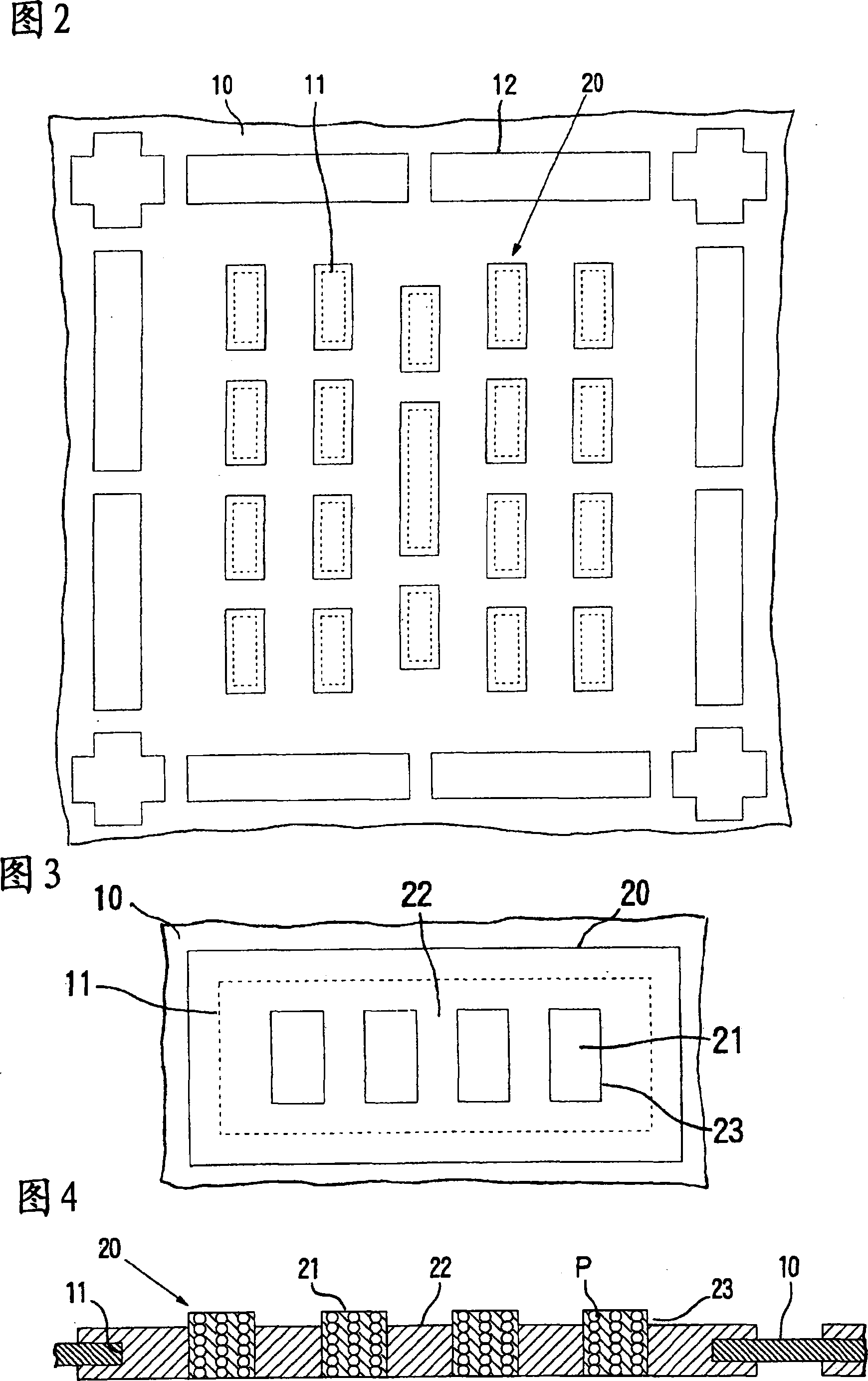
[0249] (1) In the anisotropic conductive connector, in addition to the connecting conductive portion 21 , a non-connecting conductive portion not electrically connected to the inspected electrode of the wafer may be formed in the elastic anisotropic conductive film 20 . Next, an anisotropic conductive connector having an elastic anisotropic conductive film and forming a non-connection conductive portion will be described.

[0250] Fig. 19 is an enlarged plan view showing another example of the elastic anisotropic conductive film of the anisotropic conductive connector of the present invention. For the elastic anisotropic conductive film 20 of this anisotropic conductive connector, in the thickness direction (that is, the direction perpendicular to the page in FIG. A plurality of conductive parts 21 for connection are arranged in two rows accordi...

Embodiment 1

[0276] [Production of frame board]

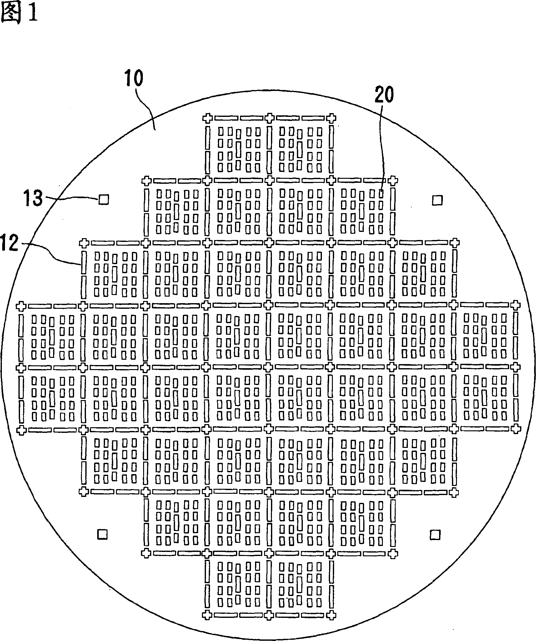
[0277] According to the structure shown in Fig. 26 and Fig. 27, according to the following conditions, the frame plate (10) with a diameter of 8 inches (10) having 393 openings (11) formed corresponding to each inspected electrode region of the above-mentioned test wafer W1 was produced.

[0278] The frame plate (10) is made of Kovar iron-nickel-cobalt alloy (linear thermal expansion coefficient 5×10 -6 / K), and its thickness is 60 μm. The openings (11) of the frame plate (10) each have a horizontal (left-right direction in FIGS. 26 and 27 ) dimension of 5.5 mm and a longitudinal (vertical direction in FIGS. 26 and 27 ) dimension of 0.4 mm.

[0279] A circular air circulation hole (12) with a diameter of 1mm is formed at the center between longitudinally adjacent openings (11).

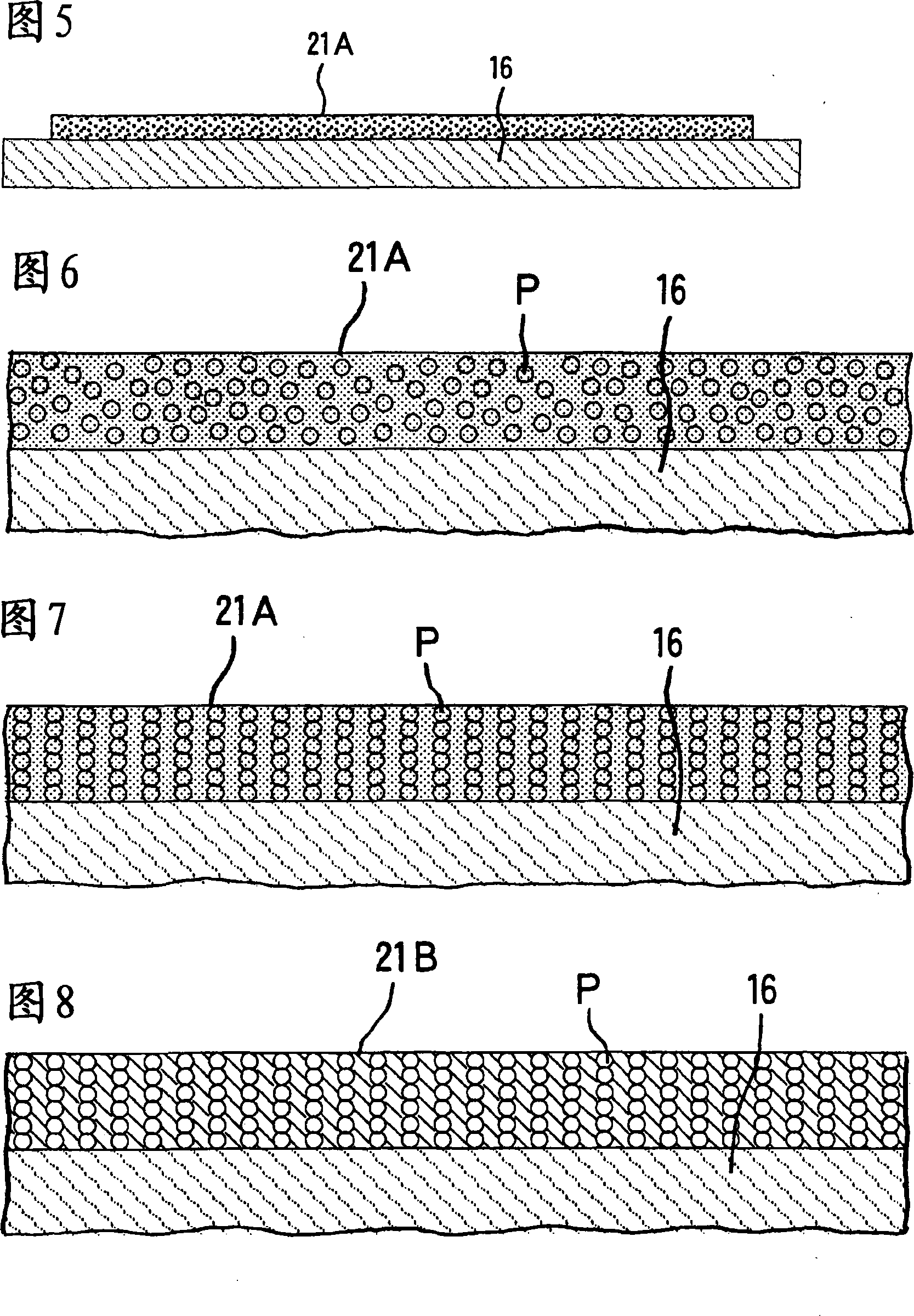
[0280] [Manufacturing of spacers for molding]

[0281] Two spacers for forming an elastic anisotropic conductive film having a plurality of openings formed corr...


PUM


Abstract

A wafer inspection-use anisotropic conductive connector capable of positively ensuring a required electrical connection even if the electrodes to be inspected of the wafer are disposed at small pitches and high density, and being produced at low costs, and a production method and applications therefore. The connector comprises a frame plate formed with a plurality of openings corresponding to electrode areas where the electrodes to be inspected of the wafer are disposed, and a plurality of elastic, anisotropic conductive films so disposed as to close the respective openings, wherein the elastic, anisotropic conductive films comprise a plurality of connecting conductive units disposed in conjunction with the electrodes to be inspected, extending in the thickness direction, and being mutually insulated by insulating units, and can be obtained by laser-processing a conductive elastomer layer supported on a releasing type support plate to form a plurality of connecting conductive units, allowing the respective connecting conductive units to impregnate into a liquid insulating unit-use material layer formed so as to close the openings of the frame plate, and hardening the insulating unit-use material layer.

Description

technical field [0001] The present invention relates to an anisotropic conductive connector for wafer inspection to be used for electrical inspection of a plurality of integrated circuits formed on a wafer in a wafer state, and a manufacturing method thereof, and an anisotropic conductive connector for wafer inspection. A probe member for wafer inspection of a device, a wafer inspection apparatus having the probe member, and a wafer inspection method using the probe member. Background technique [0002] Generally speaking, in the manufacturing process of semiconductor integrated circuit devices, for example, a plurality of integrated circuits are formed on a wafer made of silicon, and then, by inspecting the basic electrical characteristics of each of these integrated circuits, detection of defective integrated circuits is carried out. test. Next, this wafer is cut to form a semiconductor chip, and the semiconductor chip is mounted and sealed in a suitable package. Further...

Claims


Application Information

Patent Timeline
Patent Type & Authority Applications(China)
IPC IPC(8): H01L21/66H01R11/01G01R1/06G01R1/073
CPCG01R1/0735H01R12/7076H01R43/007H01R12/7082H01R13/2414H01R12/714H01L22/00
Inventor 木村洁原富士雄
Owner JSR CORPORATIOON
Why Eureka
Try Eureka