Method for manufacturing quantum dots display panel
a display panel and quantum dots technology, applied in the field of display technology, can solve the problems of not being able to be mass-produced, and achieve the effects of large-scale volume production, high-resolution graphics, and simple making process
- Summary
- Abstract
- Description
- Claims
- Application Information
AI Technical Summary
Benefits of technology
Problems solved by technology
Method used
Image
Examples
first embodiment
[0060]Specifically, shown in FIG. 5, in the quantum dots display panel of the step 4 the backlight used in the display device is blue. Backlight module 2 emits blue backlight. While the blue backlight is exciting, the quantum dots layer 14 mixing with the red and green quantum dots is emitting the red and green mixed light with the narrow FWHM. The mixed light is then passed through the red colored barrier layer 131, the green colored barrier layer 132, then is filtered into the high-purity red monochromatic light and the green monochromatic light to display red and green. The transparent light resistance layer 133, which is not covered by the quantum dots layer, displays blue directly from the blue backlight. Finally the desired red, green, and blue color by the color display is provided, and the display color gamut index is effectively improved. The quantum dots layer 14 does not include blue quantum dots material, but it uses the blue backlight matched with the transparent light ...
second embodiment
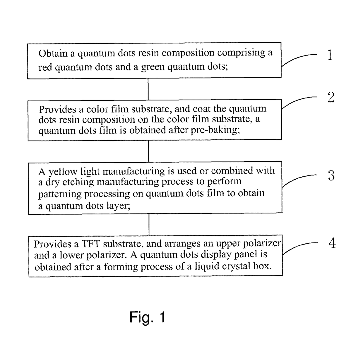
[0065]In the method for manufacturing quantum dots display panel according to the present disclosure, the step 3 of combining the yellow light manufacturing process with the dry etching manufacturing process to perform patterning processing on the quantum dots film 14′, the step 3 specifically including the steps of:
[0066]Step 31′, after pre-baking in step 2, baking the color film substrate at a temperature of 200-250 DEG C. to fully cure the quantum dots film 14′;
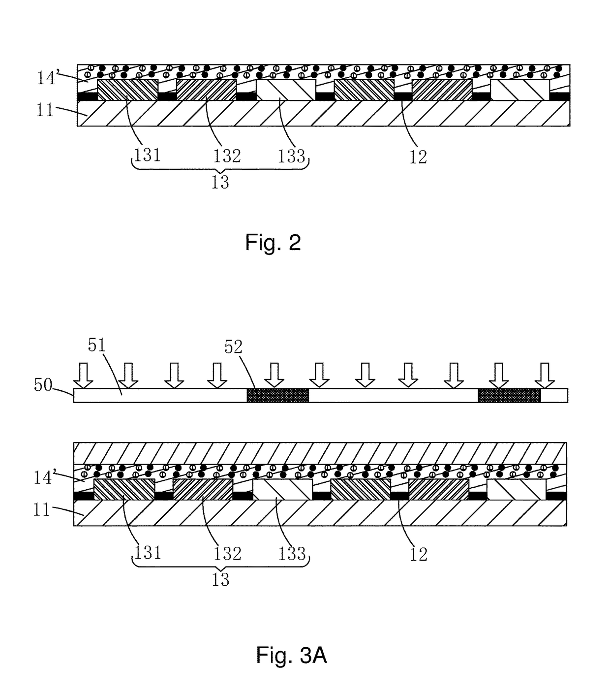
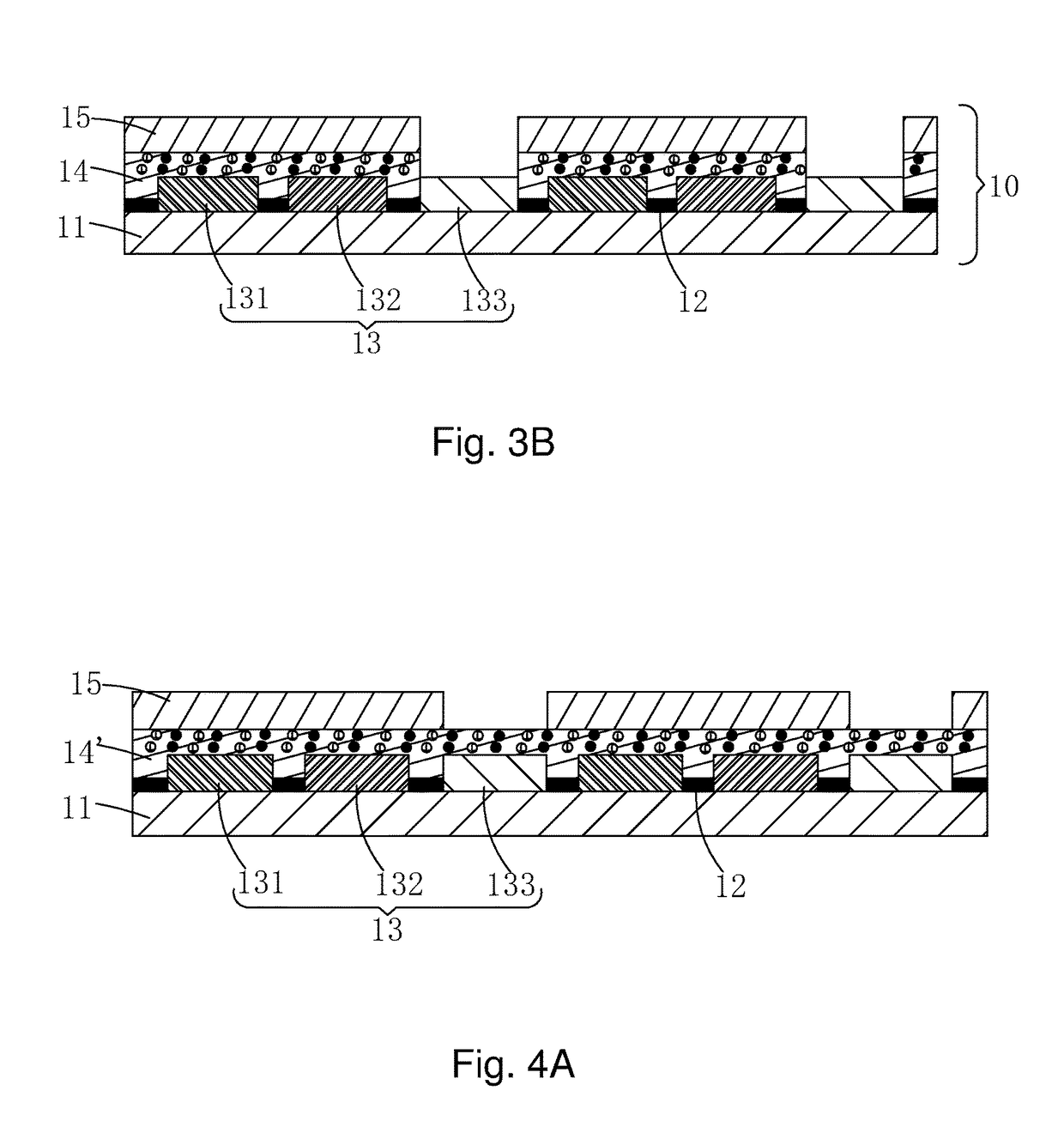
[0067]Step 32′, using a spin coating method or a slit coating method to coat a layer of transparent photoresist material (such as W photoresist, PFA photoresist) uniformly on the quantum dots film 14′ after pre-baking; providing a light mask 50, and using the light mask 50 to perform development process and exposure process of the transparent photoresist material to obtain a patterned photoresist layer 15; wherein the light mask 50 includes a transmitting portion 51 corresponding to the red colored barrier layer 131 and th...
PUM
| Property | Measurement | Unit |
|---|---|---|
| temperature | aaaaa | aaaaa |
| temperature | aaaaa | aaaaa |
| temperature | aaaaa | aaaaa |
Abstract
Description
Claims
Application Information


