Chip resistor element

a technology of resistor elements and chips, applied in the direction of resistor housing/enclosement/embedding, sustainable manufacturing/processing, final product manufacturing, etc., can solve the problems of difficult to secure a high level of conductivity, loss of performance reduced reliability of chip resistor elements, etc., to achieve excellent plating properties, strong adhesion, and low structure

Active Publication Date: 2018-10-16
SAMSUNG ELECTRO MECHANICS CO LTD
View PDF23 Cites 2 Cited by
  • Summary
  • Abstract
  • Description
  • Claims
  • Application Information

AI Technical Summary

Benefits of technology

[0007]An aspect of the present disclosure may provide a chip resistor element having an electrode protection layer having an excellent plating property and strong adhesion to a lower structure.

Problems solved by technology

In general, when a chip resistor element is used for a long period of time while exposed to an external environment, an undesired reaction may be generated in a component such as an internal electrode of the chip resistor element, such that reliability of the chip resistor element may be decreased or performance of the chip resistor element may be lost.
For example, a metal such as silver (Ag), commonly used as a material of the internal electrode, may be easily sulfurized to form an undesirable reactant (for example, Ag2S) and cause disconnections.
However, in this method, it is difficult to secure a high level of conductivity, and plating properties may be degraded, such that a plating layer for an external electrode may not be properly formed or adhesion strength thereof with respect to a lower structure may be reduced, such that a problem such as delamination may occur.

Method used


Image

  • Chip resistor element
  • Chip resistor element
  • Chip resistor element

Examples


##ventive example 1

INVENTIVE EXAMPLE 1

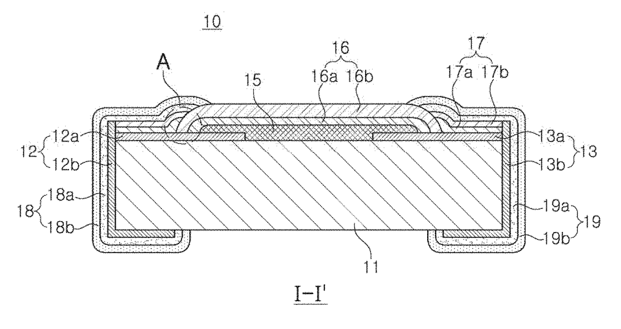
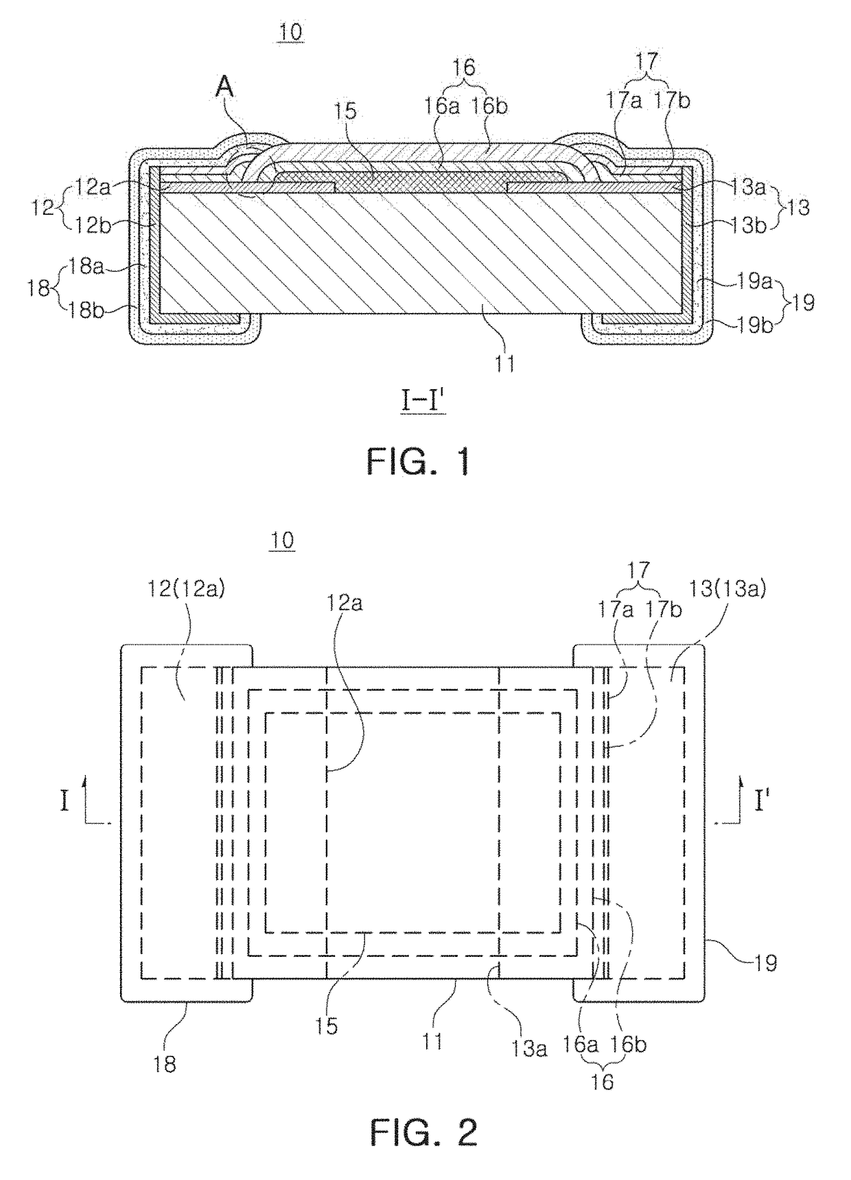
[0067]First and second electrode protection layers (e.g., 17a and 17b) were manufactured in a chip resistor element similar to the chip resistor element illustrated in FIG. 1 depending on a condition of the present disclosure.

[0068]First, upper electrodes (e.g., 12a and 13a) were formed using a paste containing Ag as a main component. The first electrode protection layer (e.g., 17a ) was formed using a paste in which carbon nanotubes and an epoxy resin were mixed with each other in a weight ratio of 3:97. As the carbon nanotubes, a product having a diameter of about 8 nm and a length of 10 μm to 15 μm was used. The second electrode protection layer (e.g., 17b) was formed on the first electrode protection layer (e.g., 17a) using a paste in which a CuNi alloy (Ni: 70 wt %), carbon nanotubes, and an epoxy resin were mixed with each other in a ratio of 94:1:5. Then, external electrodes (e.g., 18, 19) were formed by continuously performing Ni plating and Sn plating.

##ventive example 2

Inventive Example 2

Evaluation of CuNi Alloy

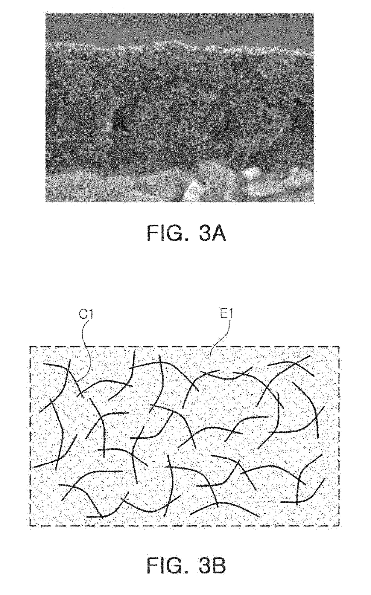
[0077]An evaluation for a CuNi alloy that may be usefully adopted in the present exemplary embodiment was performed. Sulfuration resistance characteristics and specific resistance values of alloy powder particles for the respective samples were measured while changing a ratio between Cu and Ni (a content of Ni: 0 wt %, 20 wt %, 45 wt %, 80 wt %, 100 wt %). An electrode protection layer (e.g., 17) was manufactured by mixing 90 wt % of alloy powder particles having compositions depending on the condition described above with 10 wt % of epoxy resin. The electrode protection layer manufactured in the present experiment may be a second electrode protection layer (e.g., 17b).

[0078]First, an FoS test depending on an alloy ratio was performed on the respective samples. The FoS test was performed by the same method as the method described above. Additionally, changes of specific resistance values of the respective samples depending on an amount of a...


PUM


Abstract

A chip resistor element includes an insulating substrate, a resistor layer, first and second internal electrodes, a resistor protection layer, first and second electrode protection layers, and first and second external electrodes. The resistor layer is on the insulating substrate, the first and second internal electrodes are on respective sides of the resistor layer, and the resistor protection layer covers the resistor layer and extends onto portions of the internal electrodes. The first electrode protection layers are on the first and second internal electrodes so as to overlap with portions of the resistor protection layer and contain first conductive powder particles and resin, while the second electrode protection layers are disposed on the first electrode protection layers and contain second conductive powder particles and resin. A content of resin in the second electrode protection layer is lower than in the first electrode protection layer.

Description

CROSS-REFERENCE TO RELATED APPLICATION(S)[0001]This application claims benefit of priority to Korean Patent Application No. 10-2016-0002698 filed on Jan. 8, 2016 in the Korean Intellectual Property Office, the disclosure of which is incorporated herein by reference in its entirety.BACKGROUND[0002]1. Field[0003]The present disclosure relates to a chip resistor element.[0004]2. Description of Related Art[0005]In general, when a chip resistor element is used for a long period of time while exposed to an external environment, an undesired reaction may be generated in a component such as an internal electrode of the chip resistor element, such that reliability of the chip resistor element may be decreased or performance of the chip resistor element may be lost. For example, a metal such as silver (Ag), commonly used as a material of the internal electrode, may be easily sulfurized to form an undesirable reactant (for example, Ag2S) and cause disconnections.[0006]Conventionally, a method ...

Claims


Application Information

Patent Timeline
Patent Type & Authority Patents(United States)
IPC IPC(8): H01C1/02H01C7/18H01C17/00H01C17/28H01C1/148H05K1/18H01C7/00H01C17/02H01C1/01H01C17/24H05K3/34
CPCH05K1/181H01C1/148H01C7/001H01C7/18H01C17/006H01C17/28H01C17/02Y02P70/611H01C1/01H01C17/24H05K3/3442H05K2201/10022H01C1/034H01C1/142H01C7/003Y02P70/50
Inventor YUN, JANG SEOKKIM, HYUNG MINHAN, JIN MAN
Owner SAMSUNG ELECTRO MECHANICS CO LTD
Why Eureka
Try Eureka