Thermal oxide equivalent low temperature ALD oxide for dual purpose gate oxide and method for producing the same

a technology of ald oxide and thermal oxide, which is applied in the field of manufacturing of semiconductor devices, can solve the problems of increasing unsuitability of conventional gate stacks

Active Publication Date: 2018-10-23
GLOBALFOUNDRIES US INC
View PDF10 Cites 264 Cited by
  • Summary
  • Abstract
  • Description
  • Claims
  • Application Information

AI Technical Summary

Problems solved by technology

Conventional gate stacks have become increasingly unsuitable due to uncontrolled fin to fin spacing, breakdown voltage (Vbd) deterioration, and bridge defect as the gate dielectric is thinned proportionally to the decreased gate length.

Method used


Image

  • Thermal oxide equivalent low temperature ALD oxide for dual purpose gate oxide and method for producing the same
  • Thermal oxide equivalent low temperature ALD oxide for dual purpose gate oxide and method for producing the same
  • Thermal oxide equivalent low temperature ALD oxide for dual purpose gate oxide and method for producing the same

Examples


Embodiment Construction

[0016]In the following description, for the purposes of explanation, numerous specific details are set forth in order to provide a thorough understanding of exemplary embodiments. It should be apparent, however, that exemplary embodiments may be practiced without these specific details or with an equivalent arrangement. In other instances, well-known structures and devices are shown in block diagram form in order to avoid unnecessarily obscuring exemplary embodiments. In addition, unless otherwise indicated, all numbers expressing quantities, ratios, and numerical properties of ingredients, reaction conditions, and so forth used in the specification and claims are to be understood as being modified in all instances by the term “about.”

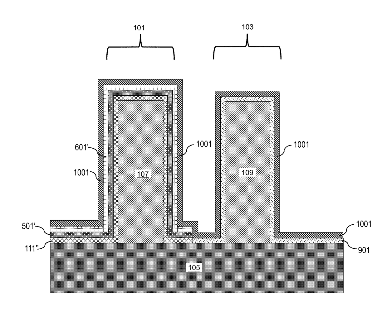
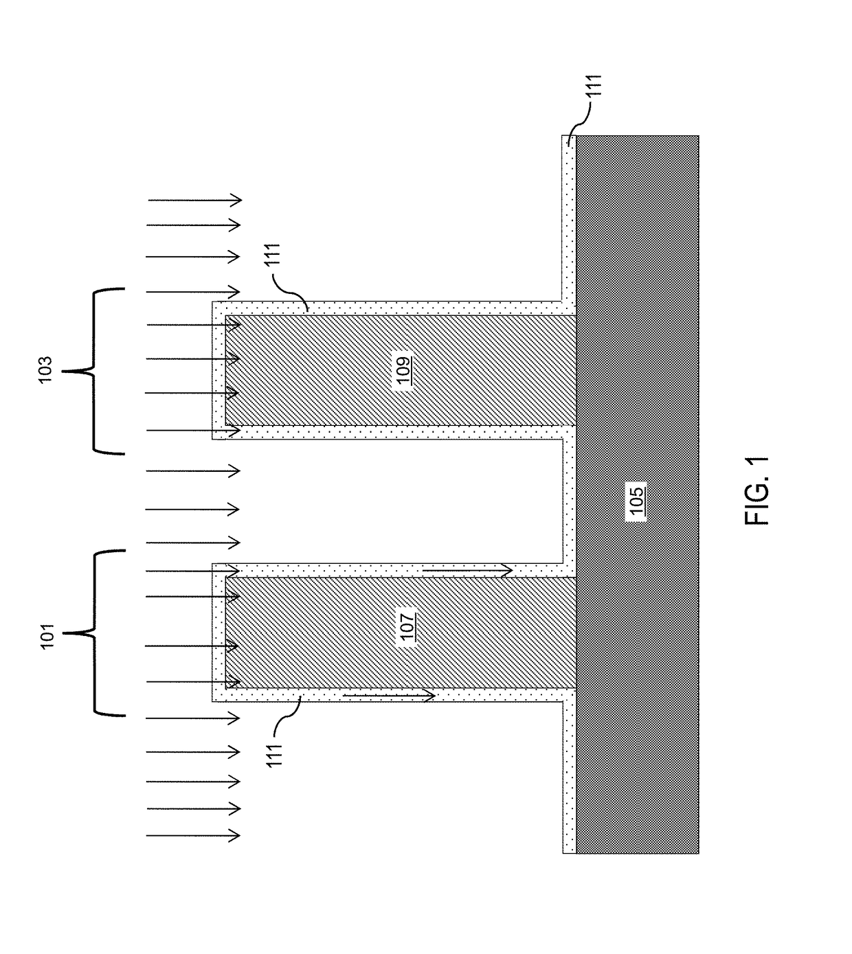
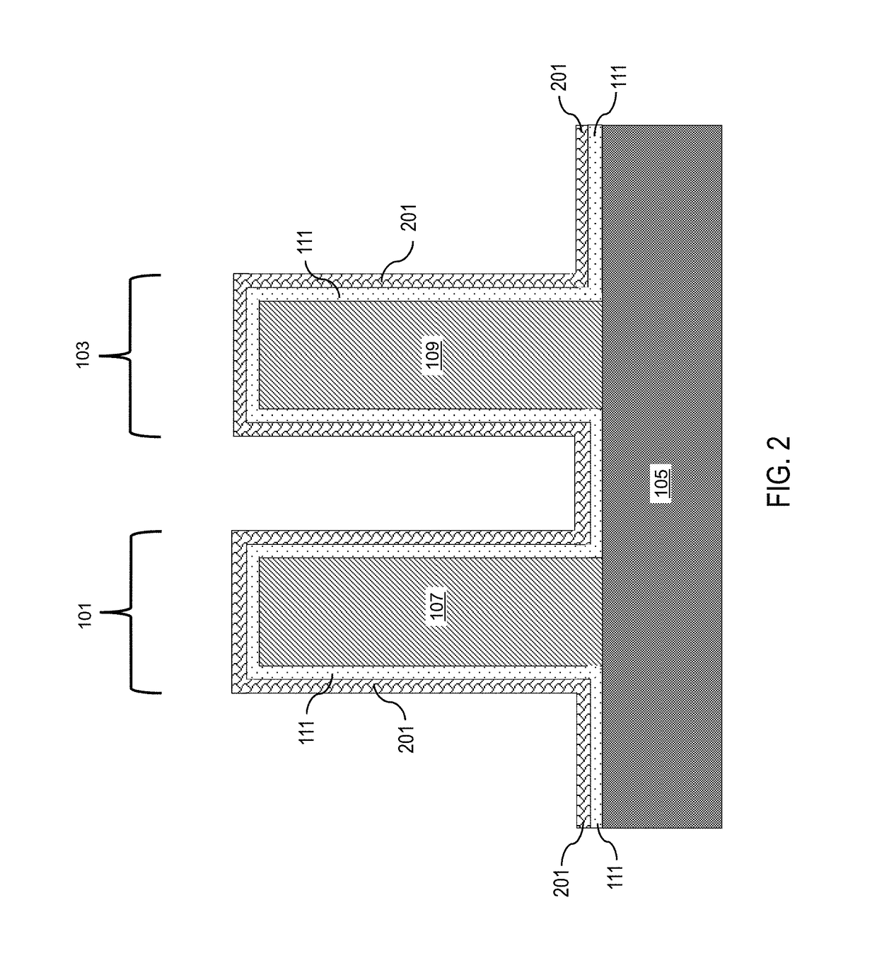
[0017]The present disclosure addresses and solves the current problems of fin to fin spacing, bridge defects, and uncontrolled Vbd and inversion layer capacitance (Cinv) attendant upon forming conformal low temperature oxides as gate oxides. The proble...


PUM

PropertyMeasurementUnit
temperatureaaaaaaaaaa
thicknessaaaaaaaaaa

Abstract

Methods of forming conformal low temperature gate oxides on a HV I / O and a core logic and the resulting devices are provided. Embodiments include providing a HV I / O and core logic laterally separated on a Si substrate, each having a fin; forming a gate oxide layer over each fin and the Si substrate; forming a silicon oxy-nitride layer over the gate oxide layer; forming a sacrificial oxide layer over the silicon oxy-nitride layer; removing the sacrificial oxide and silicon oxy-nitride layers and thinning the gate oxide layer; forming a second gate oxide layer over the thinned gate oxide layer; forming a silicon oxy-nitride layer over the second gate oxide layer; removing the silicon oxy-nitride and second gate oxide layers over the core logic fin portion; forming an IL over the core logic fin portion; and forming a HfOx layer over the second silicon oxy-nitride layer and ILs.

Description

TECHNICAL FIELD[0001]The present disclosure relates to the manufacture of semiconductor devices, such as integrated circuits (ICs). The present disclosure is particularly applicable to replacement metal gates (RMGs), particularly for the fin field-effect transistor (FINFET) based 7 nanometer (nm) technology node and beyond.BACKGROUND[0002]As the dimensions of ICs decrease, the thickness of the gate oxide is reduced to maintain performance with the decreased gate length. Conventional gate stacks have become increasingly unsuitable due to uncontrolled fin to fin spacing, breakdown voltage (Vbd) deterioration, and bridge defect as the gate dielectric is thinned proportionally to the decreased gate length.[0003]A need therefore exists for methodology enabling conformal low temperature oxide as a gate oxide for scaled FINFET.SUMMARY[0004]An aspect of the present disclosure is a method of forming conformal low temperature gate oxide on a high voltage input / output (HV I / O) and a core logic...

Claims


Application Information

Patent Timeline
Patent Type & Authority Patents(United States)
IPC IPC(8): H01L21/02C01B21/06C01B33/149H01L21/306C23C16/455C01F17/00C01F7/02
CPCC23C16/45536H01L21/0228H01L21/30604C01B33/149C01B21/0602C01F7/02C01F17/0043C01B21/0825C23C16/402C23C16/56H01L21/02164H01L21/02274H01L21/02332H01L21/0234H01L21/823431H01L21/823462H01L27/0886H01L29/66795C23C16/045
Inventor SIDDIQUI, SHAHABZAINUDDIN, ABU NASERBAUMERT, BETHUPPAL, SURESH
Owner GLOBALFOUNDRIES US INC
Why Eureka
Try Eureka