Semiconductor memory device

a memory device and semiconductor technology, applied in semiconductor devices, digital storage, instruments, etc., can solve the problems of difficult current sram architecture to produce desirable patterns, and achieve the effects of reducing inconsistent currents in different regions, enhancing performance of outer access transistors, and enhancing performance of inner transistors

Active Publication Date: 2018-11-20
UNITED MICROELECTRONICS CORP
View PDF11 Cites 8 Cited by
  • Summary
  • Abstract
  • Description
  • Claims
  • Application Information

AI Technical Summary

Benefits of technology

[0004]It is one of the primary objectives of the present invention to provide a semiconductor memory device having asymmetric two access transistors, so as to improve the inconsistent Iread and static noise margin (SNM) in different regions. In this way, the semiconductor memory device of the present invention may therefore obtain preferable quality and elemental performance.
[0006]Overall, a semiconductor memory device is provided to have asymmetric access transistors, to as to improve the aforementioned issues. Through the present invention, the performance of an outer access transistor is enhanced, and / or the performance of an inner transistor is reduced, either through changing the channel widths, the resistances or the threshold voltages thereof. That is, the currents passed through the outer access transistor and the inner access transistor may be enhance and / or reduced accordingly. In this way, the inconsistent currents in different regions are decreased, and the quality and the performance of semiconductor memory device can be improved thereby.

Problems solved by technology

However, as pitch of the exposure process decreases, it has been difficult for the current SRAM architecture to produce desirable patterns.

Method used


Image

  • Semiconductor memory device
  • Semiconductor memory device
  • Semiconductor memory device

Examples


Embodiment Construction

[0020]To provide a better understanding of the presented invention, preferred embodiments will be described in detail. The preferred embodiments of the present invention are illustrated in the accompanying drawings with numbered elements.

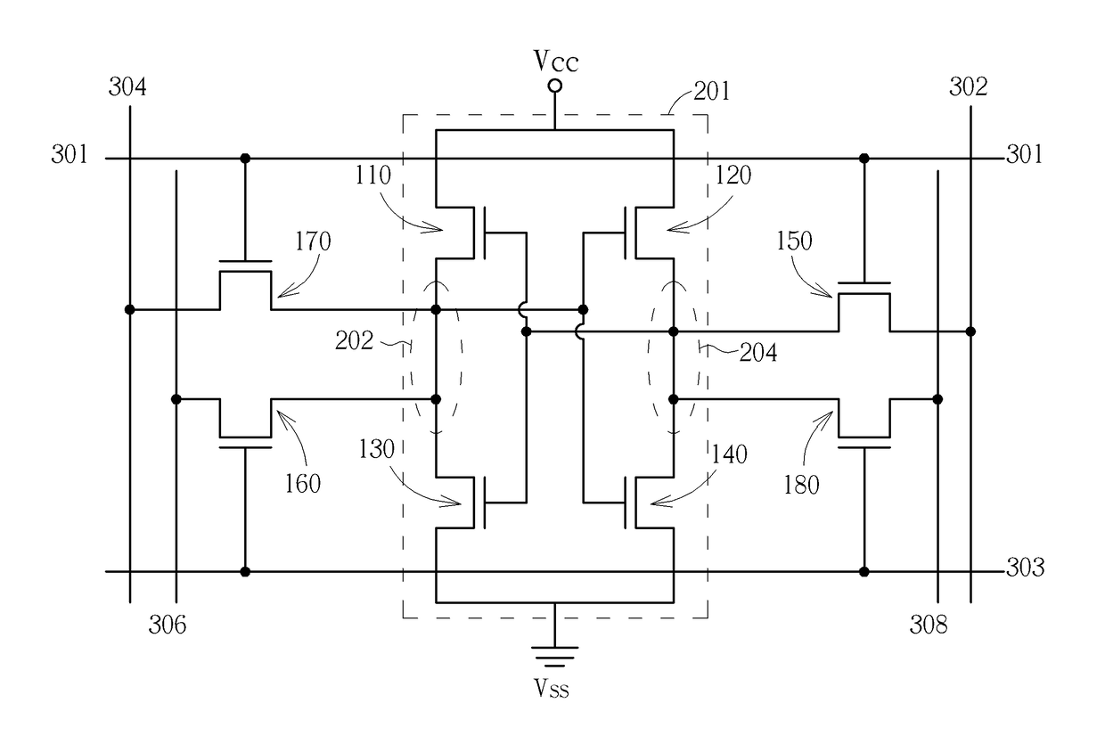
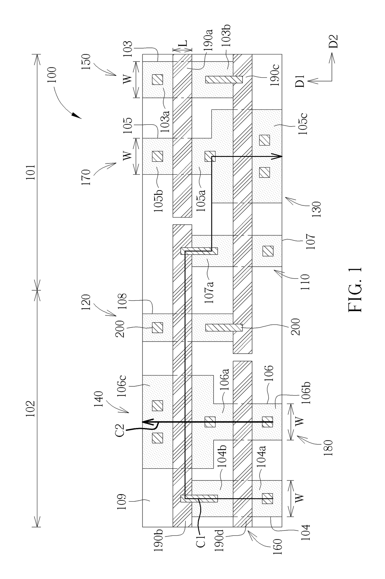
[0021]Please refer to FIG. 1 to FIG. 2, illustrating a semiconductor memory device 100, such as a static random access memory (SRAM) device, according to the first embodiment of the present invention. As shown in FIG. 1, a substrate (not shown in the drawings) such as a silicon substrate or a silicon on insulator (SOI) substrate is provided, and the substrate has a first region 101 and a second region 102 defined thereon. Also, a plurality of active areas 103, 104, 105, 106, 107, 108 parallel extended in a first direction D1, such as the y-direction, are formed on the substrate respectively, and the active areas 103, 104, 105, 106, 107, 108 are surrounded by a shallow trench isolation (STI) 109. Then, at least one gate is disposed on the substrate a...


PUM


Abstract

A semiconductor memory device includes a first inverter, a second inverter, a first and second inner access transistors, and a first and second outer access transistors. The first inverter includes a first pull-up transistor and a first pull-down transistor, the second inverter includes a second pull-up transistor (PL2) and a second pull-down transistor, and the first inverter and the second inverter forms a latch circuit. The first and second inner access transistors and the first and second outer access transistors are electrically connected to the latch circuit, and channel widths of the second inner access transistor and the second outer access transistor are different from each other.

Description

BACKGROUND OF THE INVENTION1. Field of the Invention[0001]The invention relates to a semiconductor memory device, and more particularly, to a static random access memory (SRAM) device having the advantage of improving the inconsistent currents in different regions.2. Description of the Prior Art[0002]An embedded static random access memory (SRAM) comprises a logic circuit and a static random access memory connected to the logic circuit. SRAM is a kind of volatile memory cell, which means it preserves data only while power is continuously applied. SRAM is built of cross-coupled inverters that store data during the time that power remains applied, unlike dynamic random access memory (DRAM) that needs to be periodically refreshed. Because of its high access speed, SRAM is also used in computer systems as a cache memory.[0003]However, as pitch of the exposure process decreases, it has been difficult for the current SRAM architecture to produce desirable patterns. Hence, how to enhance t...

Claims


Application Information

Patent Timeline
Patent Type & Authority Patents(United States)
IPC IPC(8): G11C11/404G11C11/417G11C11/4097H01L27/11H01L27/12
CPCH01L27/11H01L27/1211G11C11/4097G11C11/417G11C11/404G11C7/1075G11C8/16G11C11/419H01L27/0207H01L27/0924H10B10/12H10B10/00
Inventor CHEN, CHIH-HANCHEN, WEI-CHICHANG, CHINGCHEN, MING-SHINGWU, CHAO-HSIENHWANG, CHIA-HUIHUANG, LU-RAN
Owner UNITED MICROELECTRONICS CORP
Why Eureka
Try Eureka