Antenna module

a technology of antenna modules and antenna elements, applied in the field of antenna modules, can solve the problems of increased cost and difficulty in arranging antenna elements with efficiency, and achieve the effect of reducing the transmission loss between an rf chip and the antenna elements and avoiding efficiency arrangemen

Active Publication Date: 2018-11-27
PANASONIC INTELLECTUAL PROPERTY MANAGEMENT CO LTD
View PDF7 Cites 2 Cited by
  • Summary
  • Abstract
  • Description
  • Claims
  • Application Information

AI Technical Summary

Benefits of technology

[0005]One non-limiting and exemplary embodiment facilitates providing an antenna module including a plurality of antenna elements, where deficiencies in the plurality of antenna elements can be controlled, restraint-free arrangement with efficiency is enabled as well as downsizing, and transmission loss between an RF chip and the antenna elements can be decreased.
[0007]According to the present disclosure, in an antenna module including a plurality of antenna elements, deficiencies in the plurality of antenna elements can be controlled, restraint-free arrangement with efficiency is enabled as well as downsizing, and transmission loss between an RF chip and the antenna elements can be decreased.

Problems solved by technology

According to the techniques described in Japanese Unexamined Patent Application Publication (Translation of PCT Application) No. 2008-524845, however, when a plurality of antenna elements formed of wiring patterns are arranged on an outer layer of a board, the arrangement needs to avoid vias with a coaxial structure and it is thus difficult to arrange the antenna elements with efficiency and costs are raised because of increase in area of the board.

Method used


Image

  • Antenna module
  • Antenna module
  • Antenna module

Examples


first embodiment

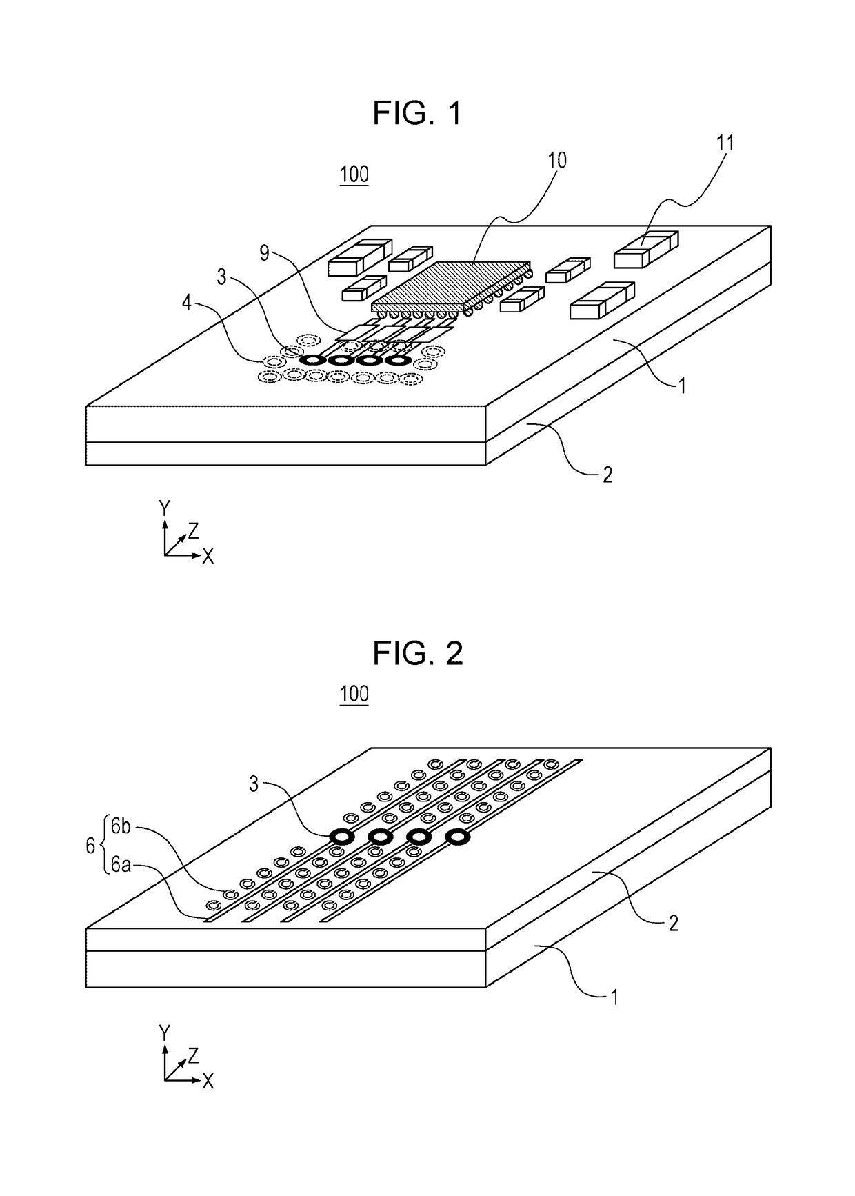
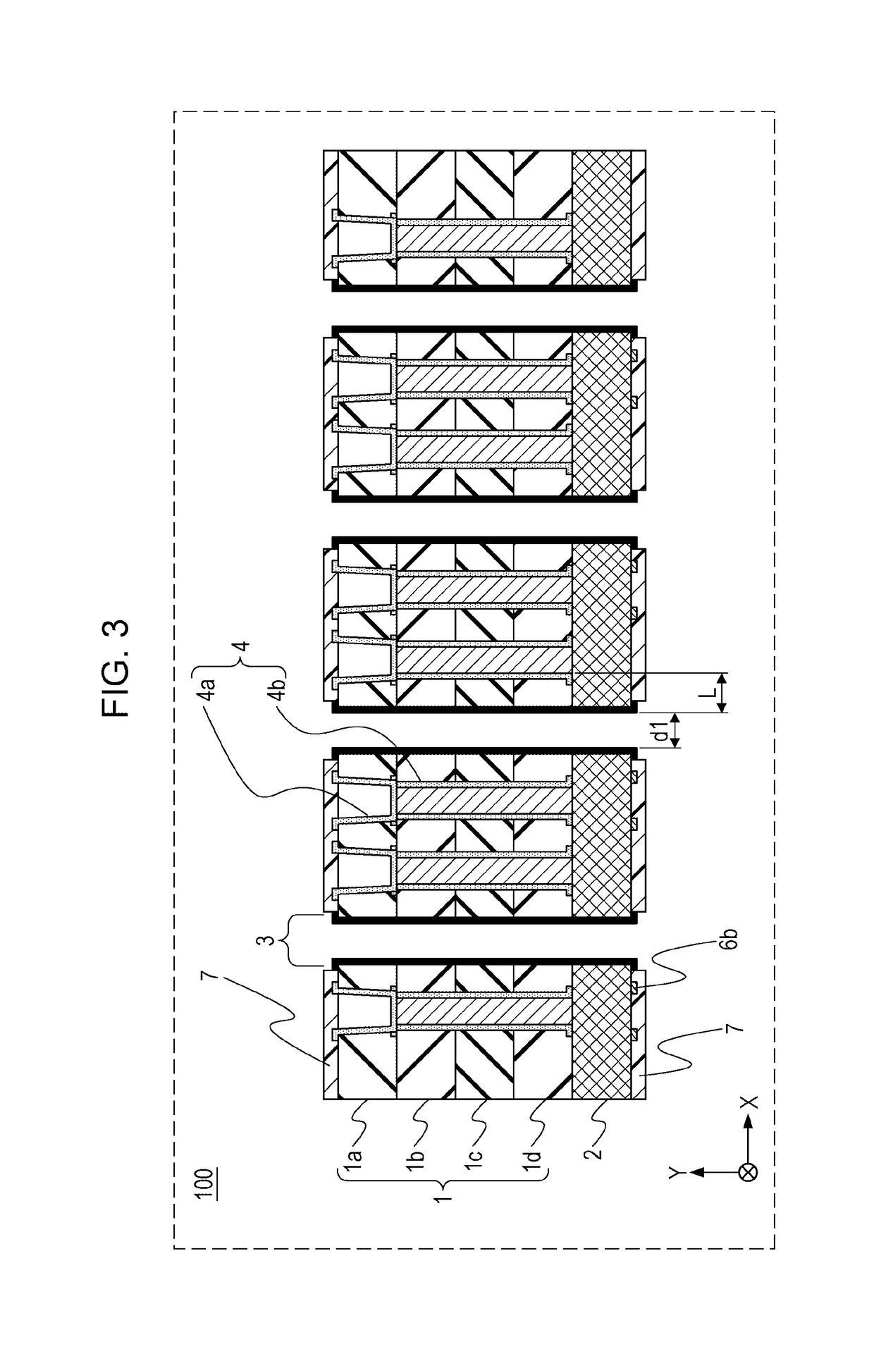
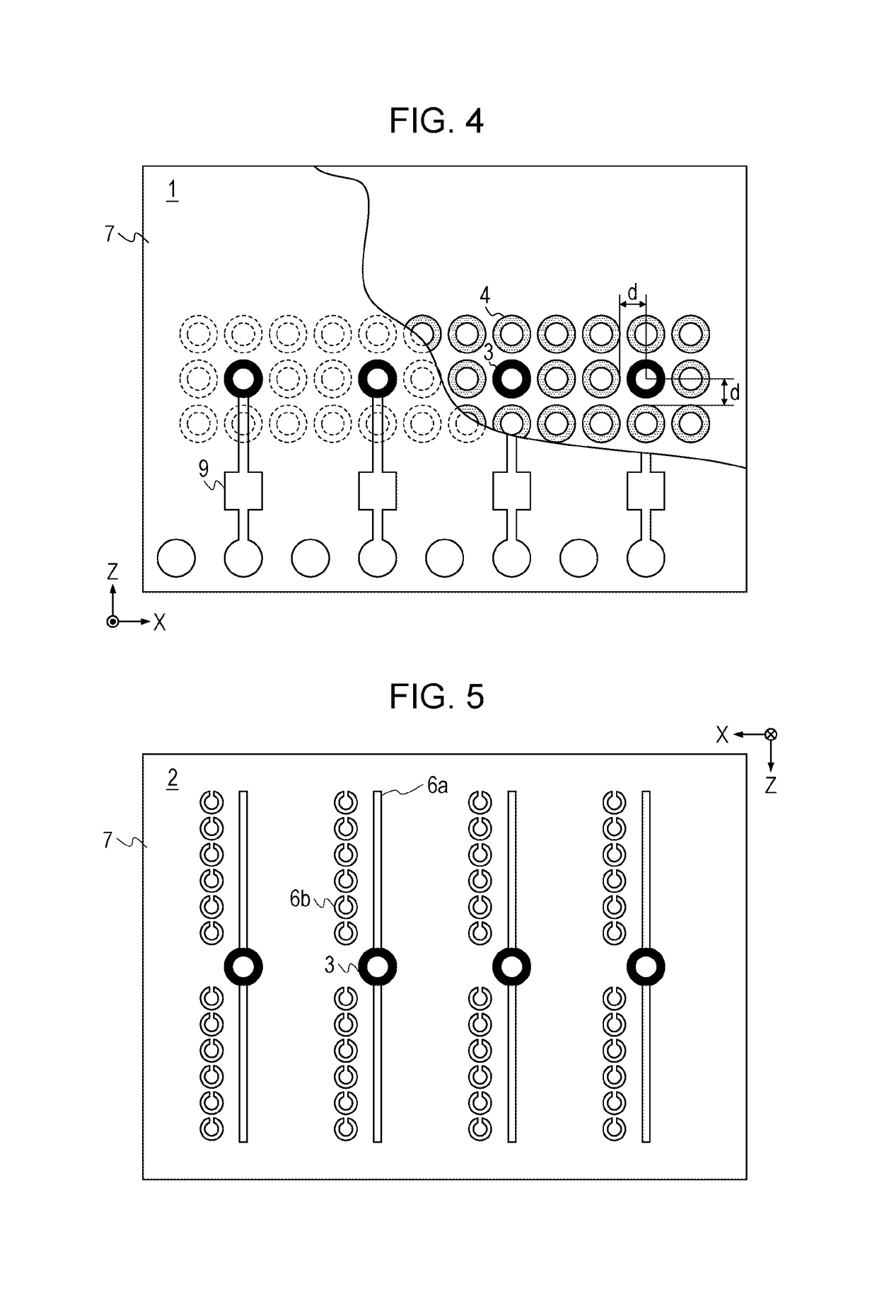
[0027]FIG. 1 is a top perspective view that illustrates an example of the configuration of an antenna module 100. FIG. 2 is a bottom perspective view that illustrates an example of the configuration of the antenna module 100. FIG. 3 is a cross-sectional view that illustrates an example of the configuration of the antenna module 100. FIG. 4 is a top view that illustrates an example of the configuration of the antenna module 100. FIG. 5 is a bottom view that illustrates an example of the configuration of the antenna module 100.

[0028]In FIGS. 1 to 5, the antenna module 100 includes a first laminate part 1, a second laminate part 2, a through hole 3, a via 4, a wiring (antenna) pattern 6, a solder resist 7, a matching circuit 9, an RF chip 10, and a circuit component 11.

[0029]In the description below, in the antenna module 100, the outer face of the first laminate part 1 is referred to as the obverse face of the antenna module 100 and the outer face of the second laminate part 2 is refe...

second embodiment

[0063]A configuration of an antenna module 200 according to a second embodiment is described below using FIGS. 7 to 9.

[0064]FIG. 7 is a cross-sectional view that illustrates an example of the antenna module 200 according to the second embodiment. FIG. 8 is a cross-sectional view that illustrates a variation of the antenna module 200 according to the second embodiment. FIG. 9 is a cross-sectional view that illustrates another variation of the antenna module 200 according to the second embodiment.

[0065]The antenna module 200 according to the second embodiment is different from the antenna module 100 according to the first embodiment in that a microvia 4a formed in an outer layer and an inner via 4b formed in an inner layer are coupled in the thickness direction (the Y axis direction) of the antenna module 200 in a step-like structure instead of being coupled on an identical axis. The other constituents in the second embodiment are the same as those of the antenna module 100 according ...

third embodiment

[0070]A configuration of an antenna module according to a third embodiment is described below.

[0071]The third embodiment describes an antenna module where the permittivity and dielectric loss in a second laminate part 2 on which a phased array antenna is formed are smaller than the permittivity and dielectric loss in a first laminate part 1 on which matching circuits 9 are arranged.

[0072]To reduce loss in the transmission from antenna elements 6b, for example, the permittivity and dielectric loss are decreased. When the antenna area for a millimeter wave band is large, transmission loss can be inhibited by using a base of low permittivity and low dielectric loss.

[0073]Since such a base of low permittivity and low dielectric loss is expensive, increase in costs for the antenna module 100 can be avoided by using a base of low permittivity and low dielectric loss for the second laminate part 2 that is smaller in capacity of a material to be used than the first laminate part 1 as descri...


PUM


Abstract

An antenna module includes a multilayer board, a phased array antenna that includes antenna elements arranged on an outer face of a second conductor layer included in the multilayer board and adjusts one or more beam directions of the antenna elements, a radio frequency (RF) chip that is arranged on an outer face of first conductor layers included in the multilayer board and outputs the radio frequency signal, a matching circuit that is arranged on the outer face of the first conductor layers and adjusts matching between impedance of the antenna elements and impedance of the RF chip, a through hole that couples the first conductor layers and the second conductor layer, and one or more vias that are on an outer side in a diameter direction of the through hole and couples the first conductor layers.

Description

BACKGROUND1. Technical Field[0001]The present disclosure relates to antenna modules and for example, relates to small-sized antenna modules that include phased array antennas, where transmission loss is decreased.2. Description of the Related Art[0002]Automobile millimeter wave radars that use the millimeter wave band of frequencies from 30 to 300 GHz have been more and more widespread in recent years. Such millimeter wave radars detect distances between the millimeter wave radars and detected objects, directions (angles) based on the millimeter wave radars where the detected objects are present, and speeds relative to the detected objects by emitting radio waves in the millimeter wave band from antennas, receiving reflected waves thereof, and processing signals. Thus, development of techniques for reducing car crashes and accidents involving pedestrians and decrease in costs are under review. Since the factors that make millimeter wave radars widespread include reduction in costs, ...

Claims


Application Information

Patent Timeline
Patent Type & Authority Patents(United States)
IPC IPC(8): H01Q21/00H01Q3/34H01Q1/38H01Q21/22H01Q9/04H05K1/02H01Q1/32H01Q21/08H05K1/03H05K3/46H01Q11/04H01Q21/06H01P5/02
CPCH01Q21/22H01Q3/34H01Q9/045H01Q9/0457H01Q21/0075H01Q21/0093H05K1/0222H05K1/0251H01Q1/38H05K3/4626H01P5/028H01Q1/3233H01Q11/04H01Q21/065H01Q21/08H05K1/0243H05K1/0373G01S7/03H01Q21/293H01Q23/00
Inventor YAMAMOTO, CHIEIWAKI, HIDEKISHIOZAKI, RYOSUKE
Owner PANASONIC INTELLECTUAL PROPERTY MANAGEMENT CO LTD
Why Eureka
Try Eureka