Wafer level electrical probe system with multiple wavelength and intensity illumination capability system

a technology of illumination capability and wafer level, which is applied in the field of wafer manufacturing, can solve the problems of not offering combined illumination/electrical performance and/or reliability tools, not reporting well controlled and calibrated light spectrum and intensity control, and not reporting tools that can conduct such experiments repeatedly

Active Publication Date: 2019-01-08
UNITED STATES OF AMERICA THE AS REPRESENTED BY THE SEC OF THE ARMY
View PDF15 Cites 2 Cited by
  • Summary
  • Abstract
  • Description
  • Claims
  • Application Information

AI Technical Summary

Benefits of technology

[0017]The present probe system enables researchers to run controlled experiments whereby the illumination wavelength and intensity can be changed. Using data from these controlled experiments, researchers can learn about the materials system of their technology and make improvements at the materials and physics level. Furthermore, the probe system enables engineers determine the way a device, circuit, prototype, or product acts under a very specific wavelength (or wavelength mix) and intensity (for quality assurance purposes). With multiple wavelengths and intensities to select from, the probe system provides the ability to deliver an extremely accurate known spectrum of light and intensity to a wide range of devices being tested.
[0027]A blackout curtain is placed over the entire probe system setup, without touching sensitive equipment, such as the manual probers. The blackout curtain is important to the setup in that it prevents light pollution that can significantly affect the research results. A custom test software is developed to control the electrical stimulation and to measure the electrical performance via the manual wafer probers. Alignment marks are positioned throughout the probe system for accurate and efficient re-configuration and setup.
[0028]As a result, the present probe system is capable of stimulating, at the device level, both electrically and optically, and then measuring the electrical output in terms of performance and reliability.

Problems solved by technology

However, transparent electronics are sensitive to the various photonic energies of incident lights at different wavelengths.
As a result, the problem currently facing the industry in this field revolves around a better understanding of the reaction of the new technologies to illumination rich environments.
However, none of the current manual wafer probe station manufacturers offer a combined illumination / electrical performance and / or reliability tool.
Yet another manufacturer offers an “optoelectronic system” capable of probing electrically, and measuring the output of light emitting devices; however, while this conventional system may provide a solution for semiconductor emitters, it does not do so for intentional and unintentional detectors.
Still another manufacturer offers several models of manual probe stations geared at the silicon market, with a specialty tool that does not address illumination measurements.
However, neither well controlled and calibrated light spectrum and intensity control, nor tools that can conduct such experiments repeatedly, have been reported.

Method used


Image

  • Wafer level electrical probe system with multiple wavelength and intensity illumination capability system
  • Wafer level electrical probe system with multiple wavelength and intensity illumination capability system
  • Wafer level electrical probe system with multiple wavelength and intensity illumination capability system

Examples


Embodiment Construction

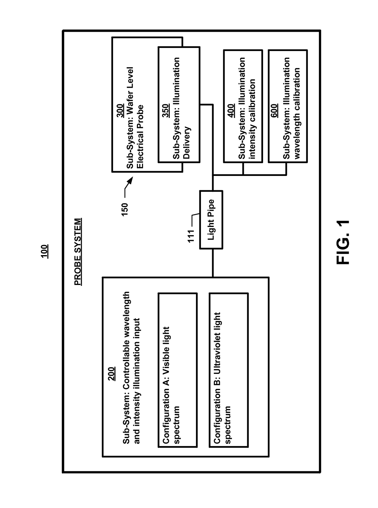
[0037]With reference to FIG. 1, it illustrates a block diagram of a probe system 100, according to a preferred embodiment of the present invention. The probe system 100 generally includes the following five sub-systems, that are interconnected by a light pipe (or light guide) 111:

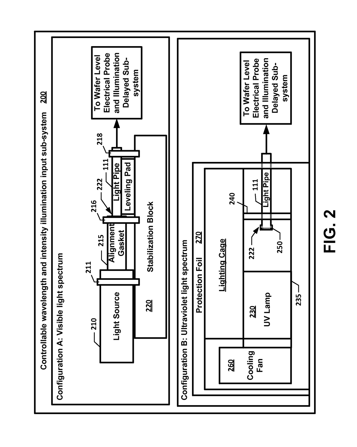
[0038](1) A controllable wavelength and intensity illumination input sub-system 200 that provides two alternative configurations:[0039]a. a visible light spectrum configuration (A); and[0040]b. an ultraviolet light spectrum configuration (B).

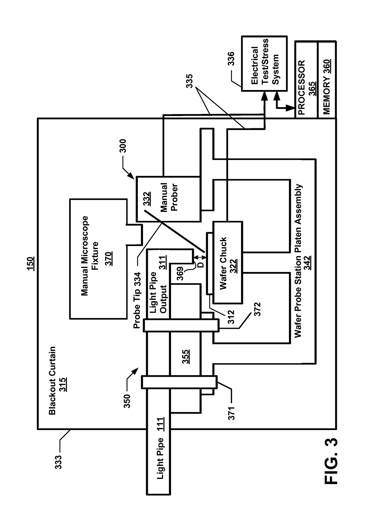
[0041](2) A wafer level electrical probe sub-system 300.

[0042](3) An illumination delivery sub-system 350.

[0043](4) An illumination intensity calibration sub-system 400.

[0044](5) An illumination wavelength calibration sub-system 600.

[0045]Considering the probe system 100 in more detail with further reference to FIG. 2, the controllable wavelength and intensity illumination input sub-system 200 is configurable into two alternative configurations:

[0046]The first is config...


PUM


Abstract

A wafer level electrical probe system with multiple wavelength and intensity illumination capability system that enables concurrent reliability studies of illumination stimulation, electrical stimulation, and the interplay of both electrical and illumination stimulation. The probe system includes five sub-systems: a controllable wavelength and intensity illumination input sub-system with two different configurations; a wafer level electrical probe sub-system; an illumination intensity calibration sub-system; an illumination delivery sub-system; and an illumination wavelength calibration sub-system.

Description

CROSS REFERENCE TO RELATED APPLICATION[0001]This application claims the benefit of U.S. Provisional Patent Application Ser. No. 61 / 978,292, filed on Apr. 11, 2014, which is incorporated herein by reference.GOVERNMENTAL INTEREST[0002]The invention described herein may be manufactured and used by, or for the Government of the United States for governmental purposes without the payment of any royalties thereon.FIELD OF THE INVENTION[0003]The present invention relates in general to the field of wafer manufacturing. Specifically, this invention relates to the testing of electronic devices on a wafer. More specifically, the present invention relates to a wafer level electrical probe system with multiple wavelength and intensity illumination capability system that enables concurrent reliability studies of illumination stimulation, electrical stimulation, and the interplay of both electrical and illumination stimulations.BACKGROUND OF THE INVENTION[0004]Conventionally, the general focus of ...

Claims


Application Information

Patent Timeline
Patent Type & Authority Patents(United States)
IPC IPC(8): G01R31/26G01R31/28G01R31/311G01R1/07G01R31/265
CPCG01R1/071G01R31/2656G01R31/309
Inventor SIDDIQUI, JEFFREY J.SANDHU, AJITLIU, JOE Y.
Owner UNITED STATES OF AMERICA THE AS REPRESENTED BY THE SEC OF THE ARMY
Why Eureka
Try Eureka