Connection substrate

a technology of connecting substrate and active metal, which is applied in the direction of printed circuit stress/warp reduction, printed element electric connection formation, etc., can solve the problems of high viscosity of metal solder containing active metal, high viscosity of metal solder, and high viscosity of active metal solder, so as to reduce the number of pores, prevent the effect of separation and deterioration of the water tightness of the separated parts

Inactive Publication Date: 2019-04-09
NGK INSULATORS LTD
View PDF36 Cites 0 Cited by
  • Summary
  • Abstract
  • Description
  • Claims
  • Application Information

AI Technical Summary

Benefits of technology

[0013]The inventors have reached the following findings in the course of studying water-tightness of the through conductor. That is, according to prior arts, a metal paste is supplied into a through hole of a ceramic substrate and then fired to obtain a through conductor. Such through conductor has the microstructure which is uniform as a whole. As the thickness of the ceramic substrate becomes extremely small, a part of open pores is communicated between both main surfaces of the through conductor, resulting in leakage of a trace amount of liquid.
[0014]Then, the inventors studied to reduce a number of pores in the metal porous body forming the through conductor. As the number of the pores of the metal porous body is small, separation at an interface between the through conductor and ceramic tends to occur due to the difference of the thermal expansions, resulting in deterioration of the water-tightness of the separated parts at which the separation occurs.
[0015]Then, the inventors focused on the microstructure of the metal porous body mainly forming the through conductor. The metal porous body includes a first open pores communicating with the first main surface and second open pores communicating with the second main surface.
[0016]Then, for preventing the separation due to the difference of thermal expansions between the through conductor and ceramics, the inventors reached the idea of generating glass phases in the respective open pores and of clogging the spaces by the glass phases in the first open pores communicating with the first main surface, so that the first open pores in the through conductor mainly provide water-tightness of the through conductor. At the same time, on the side of the second open pores communicating with the second main surface, the spaces are not clogged with the glass phase and the spaces are communicated with the second open pores. It is thus possible to preserve the water-tightness of the through conductor itself and to avoid the separation of the through conductor and ceramics as a whole, resulting in the preservation of the water-tightness also in this respect.

Problems solved by technology

Desired results are not obtained in the case that a thin substrate and a through electrode of a small size are used.
In the case that the thickness of an insulating substrate is thin, permeability of the through hole is high and the strength of the conductive protection film is insufficient so that it does not function as a protection film.
In the case that a ceramic substrate is used, however, due to a difference of thermal expansion of a metal as a conductor and ceramics, cracks or warpage of the substrate tends to occur after the substrate is thinned.
However, in addition to the problem of generation of cracks due to the difference of thermal expansion of ceramic and metal as described above, the viscosity of a metal solder containing the active metal is very high.
It is thereby difficult to fill it well in the case that the size of the through electrode is small.
It is, however, difficult to fill all the cavities only with the expansion agent.
Particularly in the case that it is thinned, the through electrode cannot be densified.
However, cracks or warping due to a difference of thermal expansions of ceramic and the powdery conductive material tends to occur.
Further, as the through hole is smaller, it becomes difficult to position the powdery conductive material.

Method used


Image

  • Connection substrate
  • Connection substrate
  • Connection substrate

Examples


example 1

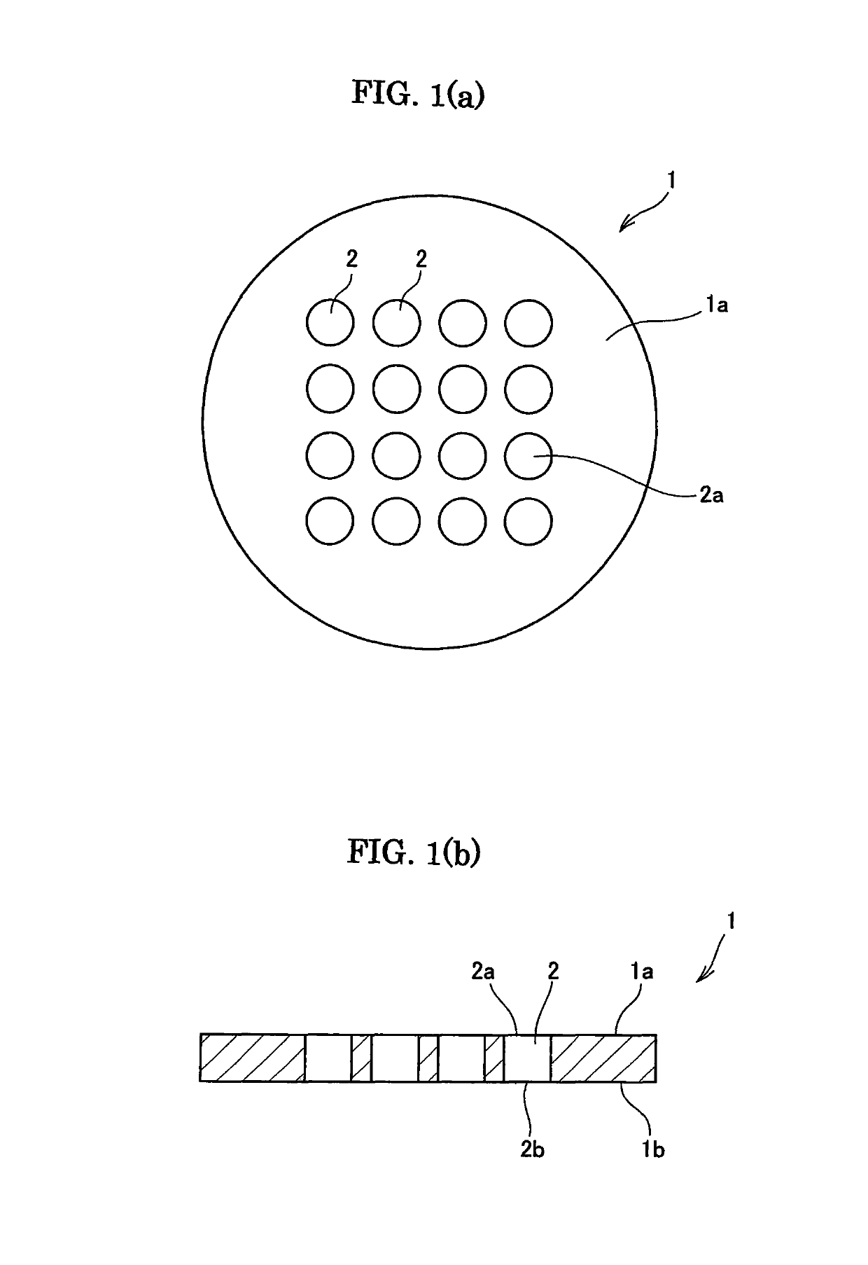
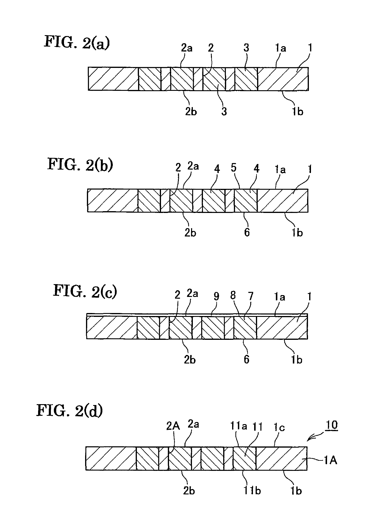
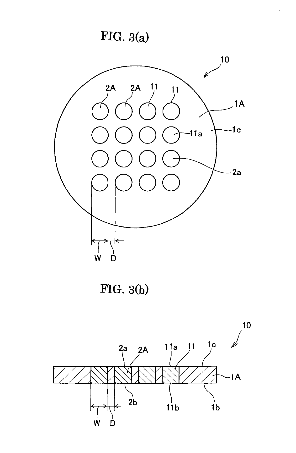
[0059]Connection substrates were produced as described referring to FIGS. 1 to 6.

[0060]Specifically, it was produced slurry by mixing the following components.

(Powdery Raw Material)

[0061]

(Powdery raw material)α-alumina powder having a specific surface area100weight partsof 3.5 to 4.5 m2 / g and an average primaryparticle size of 0.35 to 0.45 μm(alumina purity of 99.99 percent)MgO (magnesia)250ppmZrO2 (zirconia)400ppmY2O3 (yttria)15ppm(Dispersing medium)2-ethyl hexanol45weight parts(Binder)PVB (polyvinyl butyral) resin4weight parts(Dispersing agent)High molecular surfactant3weight percent(Plasticizer)DOP0.1weight parts

[0062]The slurry was then shaped into a tape by doctor blade method to a thickness corresponding with the thickness after the sintering of 300 μm, and the tape was cut into square pieces each having sizes corresponding with a length of 100 mm and a width of 100 mm after the sintering. The thus obtained powder-shaped body was calcined (preliminary sintering) in atmosphere ...

examples 2 to 7

[0092]Connection substrates were produced as the Example 1.

[0093]However, the ratio of the area of the metal porous body and the ratio (total) of the areas of the glass phases in the cross section of the through conductor were changed as shown in table 1. For changing these parameters, it was changed the concentration of the solid content of Ag—Pd paste, ratios of Ag, Pd and glass frit, sintering temperature, and temperatures and holding times during the melting and impregnation of the glass paste.

[0094]Then, as to the thus obtained ceramic substrates, it was measured the number of the through conductors with the leakage of liquid observed and shown in table 1, in 30000 counts of the through conductors provided a single ceramic substrate.

[0095]

TABLE 1Com.Ex. 1Ex. 2Ex. 3Ex. 4Ex. 5Ex. 6Ex. 7Ex. 1Number of first spaces in first open pores000000 05opening at main surface 11a (counts)Number of second spaces in second open pores658569106opening at main surface 11b (counts)Ratio of area of...


PUM

PropertyMeasurementUnit
thicknessaaaaaaaaaa
diameteraaaaaaaaaa
sizeaaaaaaaaaa

Abstract

A connection substrate includes a ceramic substrate with a through hole therein and a through conductor provided in the through hole and having first main surface and a second main surface. The through conductor includes a metal porous body having first open pores communicating with the first main surface, and second open pores communication with the second main surface, first glass phases provided in the first open pores, respectively, second glass phases formed in the second open pores, respectively, first spaces provided in the first open pores, respectively, and second spaces provided in the second open pores, respectively. The first spaces are closed spaces which do not communicate with the first main surface. The second spaces are open spaces communicating with the second main surface.

Description

CROSS-REFERENCE TO RELATED APPLICATIONS[0001]This is a continuation of International Application No. PCT / JP2017 / 003554, filed Feb. 1, 2017, which claims priority of Japanese Patent Application No. 2016-048165, filed Mar. 11, 2016, the entire contents of which are incorporated herein by reference.TECHNICAL FIELD[0002]The present invention relates to an electrical connection substrate in which a through conductor, such as a via conductor, is formed in a through hole.RELATED ART STATEMENT[0003]As a substrate for mounting an electronic device such as a SAW filter, it is used a substrate (via substrate) having the structure that a through hole is provided in an insulating substrate such as ceramic substrate and the through hole is filled with a conductor to provide a through electrode. Recently, as the reduction of size of a communication apparatus represented by cellular phone, it is demanded miniaturization and reduction of height to an electronic device used therein. It is further dem...

Claims


Application Information

Patent Timeline
Patent Type & Authority Patents(United States)
IPC IPC(8): H05K1/11H05K3/26H01L23/15H05K3/40
CPCH05K3/4061H05K3/26H01L23/15H05K1/0271H05K2201/0209H05K2201/0959H05K2203/0793H01L23/13H05K1/0306H05K1/115
Inventor MIYAZAWA, SUGIOTAKAGAKI, TATSUROIDE, AKIYOSHI
Owner NGK INSULATORS LTD
Why Eureka
Try Eureka