Metallic device for scanning near-field optical microscopy and spectroscopy and method for manufacturing same

a near-field optical microscopy and metal device technology, applied in the direction of measuring devices, scanning probe microscopy, instruments, etc., can solve the problems of aperture-snom systems exhibiting space resolution, power transmitted by optical fibers decreasing exponentially with diameter, and not yet applying snom techniques

Active Publication Date: 2019-04-30
UNIVERSIDADE FEDERAL DE MINAS GERAIS +1
View PDF17 Cites 4 Cited by
  • Summary
  • Abstract
  • Description
  • Claims
  • Application Information

AI Technical Summary

Benefits of technology

[0028]The matter dealt with herein comprises a metallic device for use preferably as a near-field optical microscopy and spectroscopy. The proposed device comprises, in general, a single body that has, at its surface, at least one trimming with adequate dimensions and details, which enable the best coupling with the electric field of the polarized light, preferably in the direction normal to the surface to be analyzed. With adjustment of the trimming position with respect to the probe apex, the device enables one to tune the absorption to the frequency of the light used in the system of the desired application, by obtaining proper conditions to generate localized surface plasmon resonance (LSPR) with specific energy, leading to the improvement of the optical efficiency. The object proposed herein has reproducibility with regard to the efficacy in optical absorption and scattering at its apex, and can analyze structures of nanometric dimensions with high resolution.

Problems solved by technology

In spite of its great application potential, the SNOM technique is not yet applied at laboratories due to the difficulty in manufacturing tips with high reproducibility, good optical efficiency, mechanical stability and nanometric apex, which parameters are indispensable to its application as probes in the SNOM system.
However, these probes have a great disadvantage: the power transmitted by the optical fiber decreases exponentially with their diameter.
For this reason, these aperture-SNOM systems exhibit space resolution on the order of from 50 to 100 nm and are still limited by applications where the analyzed signal is very intense, as for example, photoluminescence.
However, these probes from the prior art do not have reproducibility of optical efficiency.

Method used


Image

  • Metallic device for scanning near-field optical microscopy and spectroscopy and method for manufacturing same
  • Metallic device for scanning near-field optical microscopy and spectroscopy and method for manufacturing same
  • Metallic device for scanning near-field optical microscopy and spectroscopy and method for manufacturing same

Examples


example

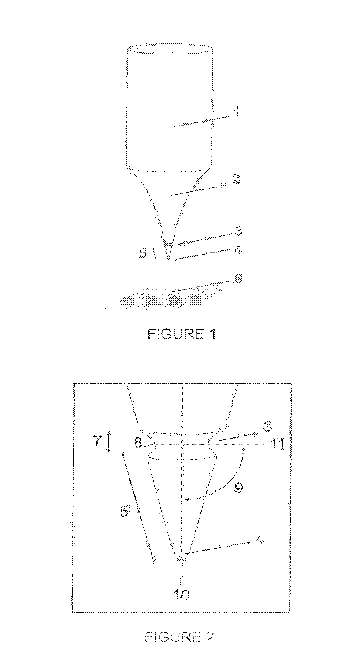
[0061]In this example one describes a process for manufacturing the metallic device with single trimming close to the nanometric end, starting from a gold probe made by electrochemical trimming of gold thread.

[0062]The manufacture of the device in the manner treated in this example is divided into three steps: (i) manufacture of the gold tip by electrochemical trimming, (ii) marking the trimming by FIB and (iii) joining to the tuning fork.

[0063]The manufacture of the gold tip may be carried out by the usual electrochemical method of trimming a gold thread, as treated in the reference: Klein, M.; Schwitzgebel, G. Review of scientific instruments 1997, 68, 3099-3103, and B. A. F. Puygranier and P. Dawson, 85 235 (2000). The gold thread should have thickness between 15 μm and 300 μm, preferably 100 μm, and exhibit purity higher than 99%, preferably higher than 99.995%. At a first moment, the thread should undergo a thermal treatment without the need to use controlled atmosphere (either...


PUM


Abstract

The present invention relates to a metallic device for near-field optical microscopy and spectroscopy, as well as to a method of preparing it. Said device comprises a single body (1) with longitudinal prolongation (2), nanometric apex (4) and has at least one trimming (3) on its surface, being applied as a probe of high optical efficiency, with adequate dimensions and details that enable the best photon-plasmon coupling, enabling the analysis, with high space resolution, of structures of nanometric dimensions with high efficiency and reproducibility.

Description

[0001]This application is the U.S. national phase of International Application No. PCT / IB2016 / 052610, filed 6 May 2016, which designated the U.S. and claims priority to BR 102015010352-2, filed 7 May 2015; the entire contents of each of which are hereby incorporated by reference.FIELD OF THE INVENTION[0002]The present invention relates to a metallic device and a method for manufacturing it, for applications in near-field microscopy and spectroscopy. More precisely, one describes a metallic device for application as a high-efficiency optical probe.BACKGROUND OF THE INVENTION[0003]Conventional optical microscopes exhibit a limited space resolution of approximately λ / 2, that is, about 300 nm in the case of visible light as a source (λ being the wavelength of the incident light). This limit is given by the Rayleigh criterion, which is defined as the separation between two punctual sources of light, so that the main maximum of diffraction of one will coincide with the first minimum of di...

Claims


Application Information

Patent Timeline
Patent Type & Authority Patents(United States)
IPC IPC(8): G01Q70/10G01Q60/22
CPCG01Q60/22G01Q70/10
Inventor DE LOURENCO E VASCONCELOS, THIAGOSOARES ARCHANJO, BRAULIODE OLIVEIRA LOPES CANCADO, LUIZ GUSTAVOACHETE, CARLOS ALBERTONUNES RODRIGUES, WAGNERJORIO DE VASCONCELOS, ADOFRAGNEAUD, BENJAMINDOS SANTOS RIBEIRO, DOUGLASRABELO E SILVA, CASSIANOSANTOS DE OLIVEIRA, BRUNO
Owner UNIVERSIDADE FEDERAL DE MINAS GERAIS
Why Eureka
Try Eureka