Methods and devices for microelectromechanical resonators

a micro-electromechanical and resonator technology, applied in the field of mems sensors, can solve the problems of increasing complexity, increasing costs, and reducing yields

Active Publication Date: 2019-05-14
MY01 IP HLDG INC
View PDF11 Cites 1 Cited by
  • Summary
  • Abstract
  • Description
  • Claims
  • Application Information

AI Technical Summary

Problems solved by technology

Generally, these increase complexity, increase costs, and reduce yields as mechanical / physical sealing of the fabricated MEMS / MEMS-CMOS circuit is required.
However, the resonating elements of the MEMS are anchored to the substrate which yields anchor damping losses arising from the transfer of kinetic energy from the resonator to its support structure.
Anchor damping can impose considerable losses in MEMS resonators and thus dramatically affect the quality factor.
However, in this design process the electrostatic transduction area has been also limited by the thickness of the material, especially where the resonator is laterally driven, that can be processed at these small dimensions).
This being addition to reduced fabrication yields and in many instances use of fabrication processes that were not amendable to mass-production.
This is essentially because of the unparalleled benefits available from CMOS in the areas of circuit size, operating speed, energy efficiency and manufacturing costs which continue to improve from the geometric downsizing that comes with every new generation of semiconductor manufacturing processes.
This power consumption arising from the charging and discharging of various load capacitances within the CMOS gates, mostly gate and wire capacitance, but also transistor drain and transistor source capacitances, whenever they are switched.

Method used


Image

  • Methods and devices for microelectromechanical resonators
  • Methods and devices for microelectromechanical resonators
  • Methods and devices for microelectromechanical resonators

Examples


Embodiment Construction

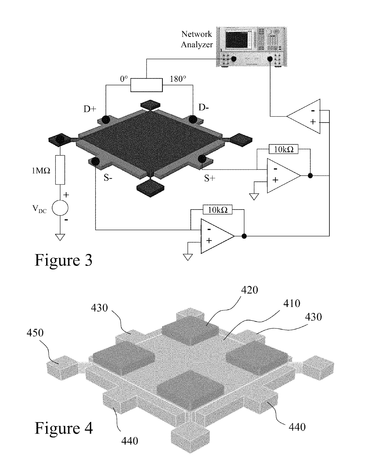
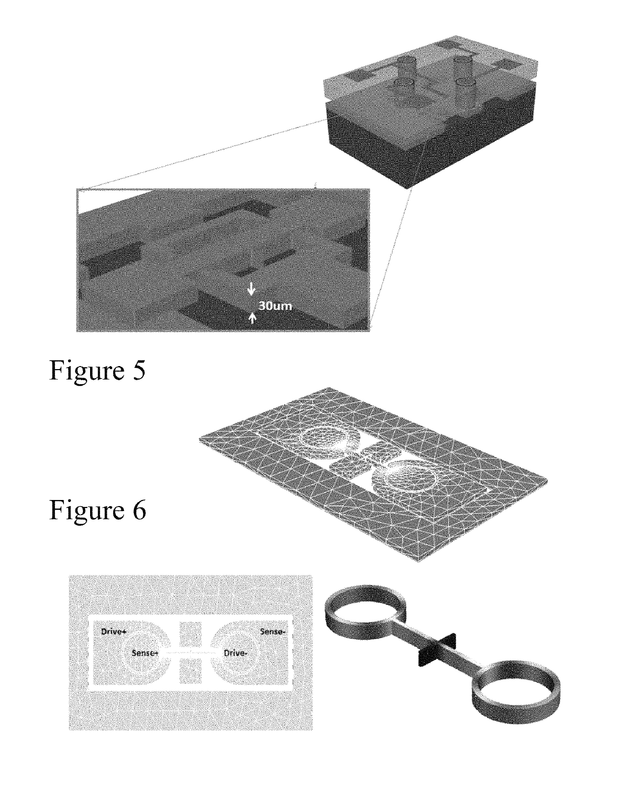
[0051]The present invention is directed to MEMS sensors and more particularly to MEMS resonators which may be manufactured directly over or in conjunction with silicon based CMOS electronics.

[0052]The ensuing description provides exemplary embodiment(s) only, and is not intended to limit the scope, applicability or configuration of the disclosure. Rather, the ensuing description of the exemplary embodiment(s) will provide those skilled in the art with an enabling description for implementing an exemplary embodiment. It being understood that various changes may be made in the function and arrangement of elements without departing from the spirit and scope as set forth in the appended claims.

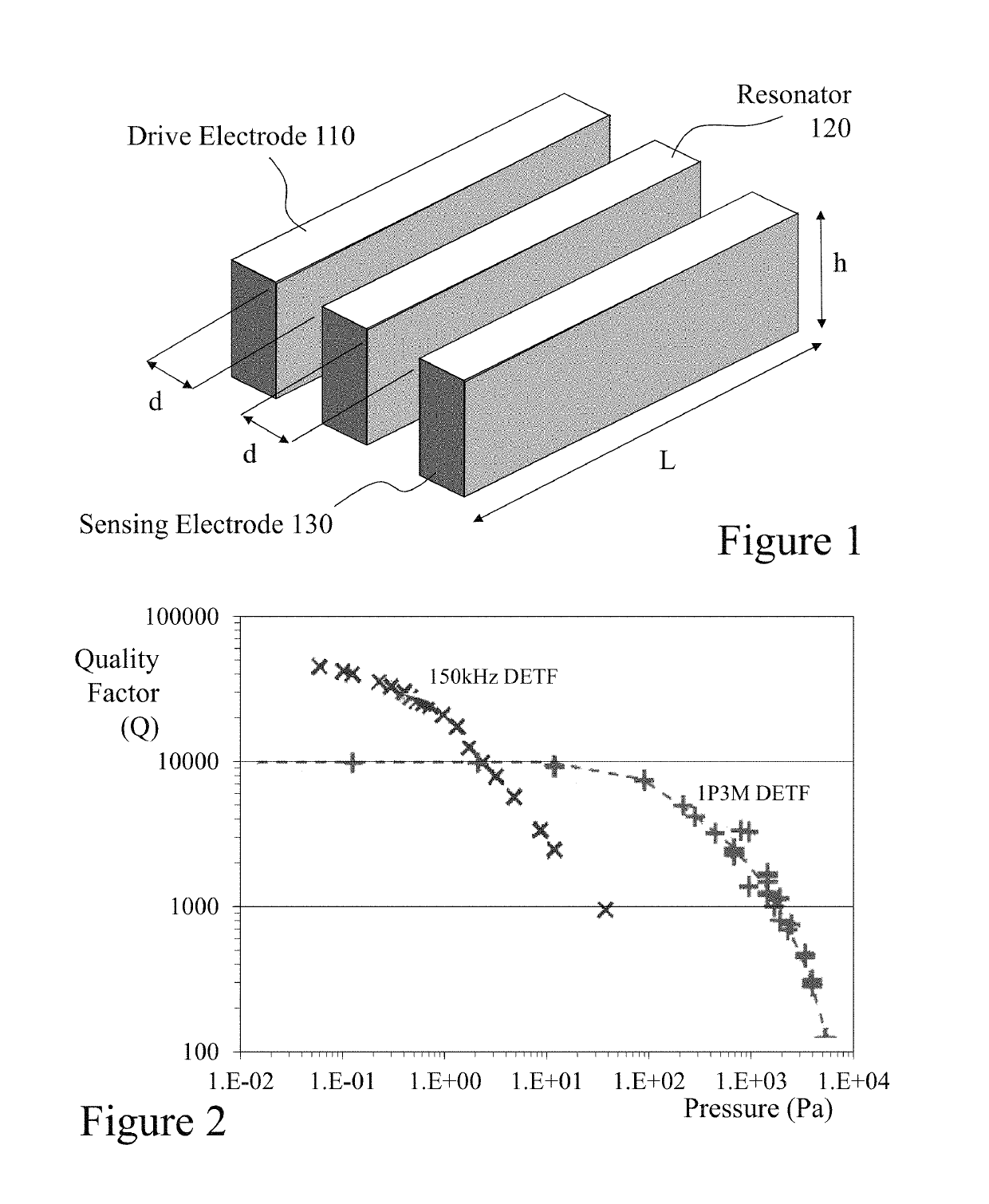
[0053]MEMS Resonator

[0054]Modern consumer electronic devices impose stringent requirements of low cost, low assembly complexity, compact system integration, high functionality, and low power consumption. Accordingly, MEMS resonators which offer reduced production costs through batch manufacturing ...


PUM

PropertyMeasurementUnit
bias voltageaaaaaaaaaa
voltageaaaaaaaaaa
pressuresaaaaaaaaaa

Abstract

MEMS based sensors, particularly capacitive sensors, potentially can address critical considerations for users including accuracy, repeatability, long-term stability, ease of calibration, resistance to chemical and physical contaminants, size, packaging, and cost effectiveness. Accordingly, it would be beneficial to exploit MEMS processes that allow for manufacturability and integration of resonator elements into cavities within the MEMS sensor that are at low pressure allowing high quality factor resonators and absolute pressure sensors to be implemented. Embodiments of the invention provide capacitive sensors and MEMS elements that can be implemented directly above silicon CMOS electronics.

Description

CROSS-REFERENCE TO RELATED APPLICATIONS[0001]This patent application claims the benefit of U.S. Provisional Patent Application 62 / 020,049 filed Jul. 2, 2014 entitled “Methods and Devices for Microelectromechanical Sensors”, the entire contents of which are included by reference.FIELD OF THE INVENTION[0002]The present invention relates to MEMS sensors and more particularly to MEMS resonators which may be manufactured directly over or in conjunction with silicon based CMOS electronics.BACKGROUND OF THE INVENTION[0003]Microelectromechanical systems (MEMS) are small integrated devices or systems that combine electrical and mechanical components. The components can range in size from the sub-micrometer level to the millimeter level, and there can be any number, from one, to few, to potentially thousands or millions, in a particular system. Historically MEMS devices have leveraged and extended the fabrication techniques developed for the silicon integrated circuit industry, namely lithogr...

Claims


Application Information

Patent Timeline
Patent Type & Authority Patents(United States)
IPC IPC(8): B81B7/00H03H9/24H03H3/007G01L9/12G01L9/00H03H9/10B81C1/00H03H9/05
CPCH03H9/1057B81C1/00182B81C1/00269B81C1/00301G01L9/0042G01L9/0073G01L9/12H03H3/0072H03H3/0073H03H9/0561H03H9/2405H03H9/2426H03H9/2431H03H9/2436B81B7/007H03H2009/2442B81B2203/0307H03H9/2452H03H9/2463H03H9/2473H03H9/2478
Inventor CHODAVARAPU, VAMSYXEREAS, GEORGE
Owner MY01 IP HLDG INC
Why Eureka
Try Eureka