Optical subassembly, optical module, and optical transmission equipment

a technology of optical sub-assembly and optical transmission equipment, applied in semiconductor lasers, printed circuit non-printed electric components association, instruments, etc., can solve the problems of sudden drop in characteristic impedance, drop in yield, and inability to provide inside the metal disk is not desirable, and achieves simple process and reduces impedance mismatch

Active Publication Date: 2019-06-25
LUMENTUM JAPAN INC
View PDF10 Cites 5 Cited by
  • Summary
  • Abstract
  • Description
  • Claims
  • Application Information

AI Technical Summary

Benefits of technology

[0009]Moreover, considering the work of soldering flexible printed circuits (FPC) mounted as an interface for electrical connection to a printed circuit board (PCB) from an optical subassembly, to a pair of differential signal terminals on the outer end faces, there is a possibility that an electrical short circuit may occur and thus cause a drop in yield, due to the very narrow space between the pair of differential signal terminals. To realize stable manufacture, a package using simple coaxial lines instead of a dual-pin structure, thus enabling relaxation of impedance mismatch, is desirable.
[0011]In view of the foregoing problems, an object of the invention is to provide an optical subassembly, an optical module, and an optical transmission equipment that can restrain impedance mismatch by a simple process.
[0023]The invention provides an optical subassembly, an optical module, and an optical transmission equipment that can restrain impedance mismatch by a simple process.

Problems solved by technology

However, the case where differential transmission lines based on the dual-pin structure disclosed in US 2014 / 0217570 A1 are provided inside the metal disk is not desirable because the characteristic impedance varies significantly due to the position where the differential signal terminals (lead terminals) are fixed, compared with simple coaxial lines.
For example, if the distance between the pair of lead terminals is short, the electrical coupling between normal phase and reversed phase is firmer, resulting in a sudden drop in characteristic impedance.
Moreover, considering the work of soldering flexible printed circuits (FPC) mounted as an interface for electrical connection to a printed circuit board (PCB) from an optical subassembly, to a pair of differential signal terminals on the outer end faces, there is a possibility that an electrical short circuit may occur and thus cause a drop in yield, due to the very narrow space between the pair of differential signal terminals.
This increases component costs, compared with when a penetration hole with a single diameter is provided.
Therefore, using the related-art techniques, it is difficult to meet the market demand for lower costs that is expected from now on.

Method used


Image

  • Optical subassembly, optical module, and optical transmission equipment
  • Optical subassembly, optical module, and optical transmission equipment
  • Optical subassembly, optical module, and optical transmission equipment

Examples


Embodiment Construction

[0032]Hereinafter, an embodiment of the invention will be described specifically and in detail, based on the drawings. In all of the drawings to explain the embodiment, members having the same functions are denoted by the same reference signs and not described repeatedly. The illustrations given below simply explain an example of embodiment. The sizes in the illustration do not necessarily coincide with the scales described in the example of embodiment.

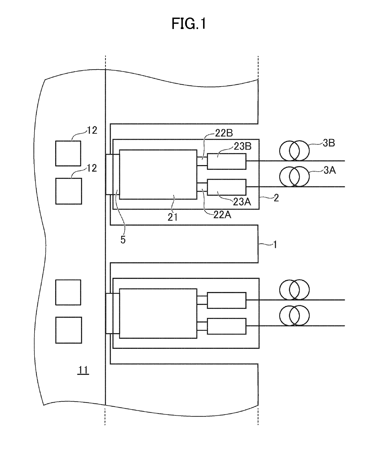
[0033]FIG. 1 is a schematic view showing the configuration of an optical transmission equipment 1 and an optical module 2 according to an embodiment of the invention. The optical transmission equipment 1 has a printed circuit board 11 (PCB) and an IC 12. The optical transmission equipment 1 is, for example, a large-capacity router or switch. The optical transmission equipment 1 has, for example, the function of a switchboard and is arranged at a base station or the like. The optical transmission equipment 1 is equipped with a pluralit...


PUM


Abstract

An optical subassembly includes: a conductor plate having a pair of penetration holes, both penetrating the conductor plate from an outer surface to an inner surface; a pair of lead terminals fixed in the two respective penetration holes and passing through the pair of penetration holes; a wiring board with a pair of wiring patterns arranged on a surface; and a plurality of bonding wires electrically connecting the pair of lead terminals and the pair of wiring patterns. A cross section of the pair of lead terminals on the inner surface side is larger than a cross section on the outer surface side. End faces on the inner surface side are situated within a range from +180 μm to −100 μm to the inner side from the inner surface of the conductor plate in a direction perpendicular to the inner surface.

Description

CROSS-REFERENCE TO RELATED APPLICATION[0001]The present application claims priority from Japanese application JP2017-085431, filed on Apr. 24, 2017, the content of which is hereby incorporated by reference into this application.BACKGROUND OF THE INVENTION1. Field of the Invention[0002]The present invention relates to an optical subassembly, an optical module, and an optical transmission equipment, and particularly to a technique for restraining impedance mismatch.2. Description of the Related Art[0003]An optical subassembly (OSA) having an optical semiconductor device has been used. Recently, not only higher speeds but also lower costs have been increasingly demanded of an optical module having one or a plurality of optical subassemblies.[0004]The optical subassembly disclosed in US 2014 / 0217570 A1 has the stem. The stem has the pair of differential signal terminals, and the metal disk on which the pair of differential signal terminals are installed. The pair of differential signal ...

Claims


Application Information

Patent Timeline
Patent Type & Authority Patents(United States)
IPC IPC(8): H05K1/18H05K1/02H05K1/14H01S5/022H05K3/10
CPCH05K1/025H01S5/02276H05K1/0274H05K1/189H05K3/103H05K1/141H05K2203/049H05K2201/10121G02B6/4274G02B6/4281H01L25/167H05K3/3447H05K3/363H01S5/02212H01S5/06226H01S5/02345
Inventor NOGUCHI, DAISUKEYAMAMOTO, HIROSHI
Owner LUMENTUM JAPAN INC
Why Eureka
Try Eureka