

Organic charge transport layer, organic EL device, organic semiconductor device, and organic photoelectric device
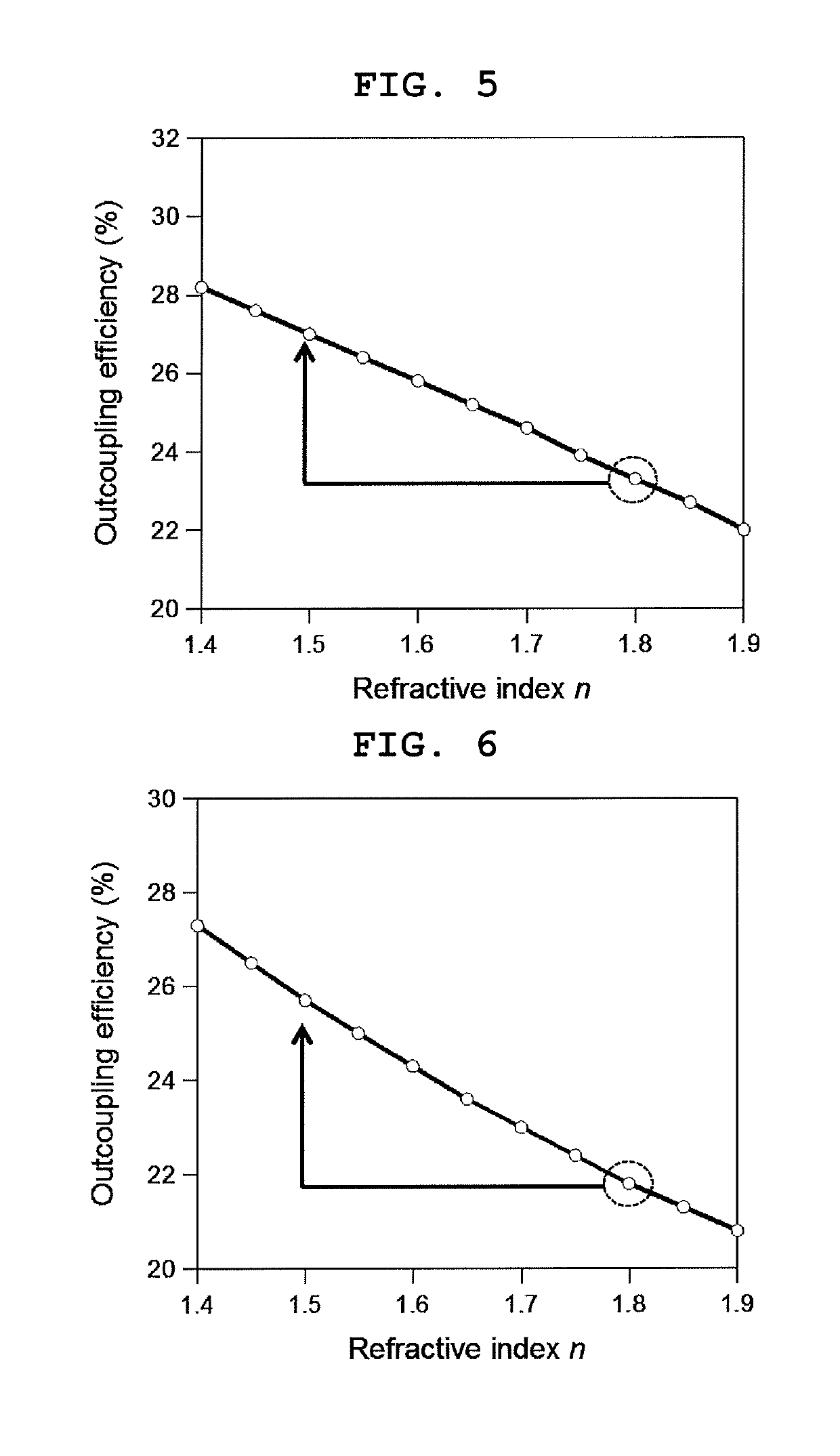
a charge transport layer and organic semiconductor technology, applied in the direction of organic conductors, non-metal conductors, luminescent compositions, etc., can solve the problems of damage to the organic semiconductor layer as a lower layer, difficulty in effective control of light propagation or outcoupling efficiency, and high cost required for the process or cost of the substrate member, so as to achieve the effect of enhancing the outcoupling efficiency of an organic el element and dramatically reducing the refractive index
- Summary
- Abstract
- Description
- Claims
- Application Information
AI Technical Summary
Benefits of technology
Problems solved by technology
Method used
Image

Examples
example 1
1. Evaluation of Refractive Index
1-1. Sample Preparation
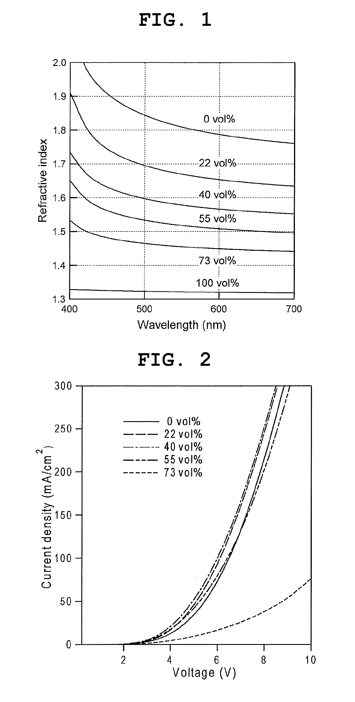
[0073]A silicon substrate cut to have about 2 cm square was subjected to ultrasonic cleaning using neutral detergent, acetone, and isopropanol. After further cleaning by boiling in isopropanol, adhered matters on a surface of the substrate were removed by an ozone treatment. The substrate was placed in a vacuum vapor deposition apparatus followed by vacuum treatment at pressure of 10−4 Pa or less. By using α-NPD as an organic semiconductor material and Teflon (registered trademark) AF1600 (manufactured by Du Pont) as an electret material such that the ratio between α-NPD and AF1600 is 100:0, 78:22, 60:40, 45:55, 27:73, or 0:100 (all in volume ratio), performing resistance heating in a vacuum vapor deposition apparatus, and performing vapor codeposition, each layer with a thickness of about 100 nm was produced. The total deposition rate for the two materials was set at 2.0 Å / s.
1-2. Measurement
[0074]By using multiple angle of inc...
example 2
1. Evaluation of Refractive Index
1-1. Sample Preparation
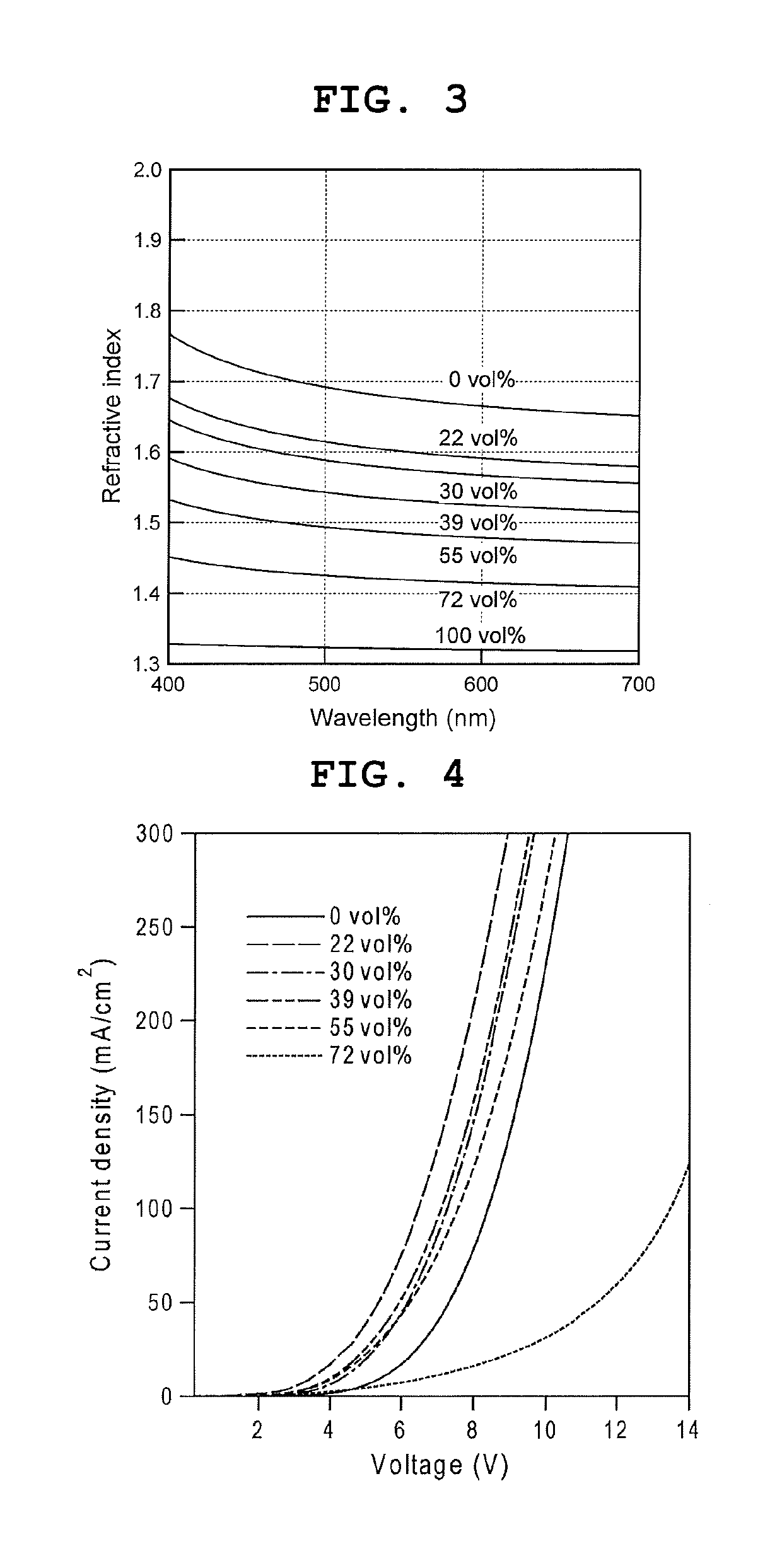
[0083]Vapor codeposition was carried out in the same manner as Example 1 except that, with regard to Example 1, TAPC was used as an organic semiconductor material and TAPC and AF1600 were used such that their ratio was 100:0, 78:22, 70:30, 61:39, 45:55, 28:72, or 0:100. As a result, a layer with thickness of about 100 nm was produced.
1-2. Measurement
[0084]The refractive index was measured in the same manner as Example 1 by using the vapor deposited film obtained in 1-1.
[0085]A change in the refractive index at a wavelength of 550 nm according to the mixing ratio of AF1600 relative to TAPC is shown in Table 2 and FIG. 3.
[0086]
TABLE 2TAPC:AF1600Refractive Index(volume ratio)(@ wavelength of 550 nm)100:0 1.6778:221.6070:301.5861:391.5345:551.4828:721.42 0:1001.32
[0087]From Table 2 and FIG. 3, it was confirmed that the refractive index of a vapor-codeposited film monotonically decreases in accordance with an increase in mixing volu...
PUM
| Property | Measurement | Unit |
|---|---|---|
| refractive index | aaaaa | aaaaa |
| internal quantum efficiency | aaaaa | aaaaa |
| refractive index | aaaaa | aaaaa |
Abstract
Description
Claims
Application Information