Method and device for cleaving wafers

a technology of cleaving and wafers, applied in the field of cleaving wafers, can solve the problems of a high percentage of material loss, and achieve the effects of enhancing heat transfer by conduction, reducing temperature, and increasing the efficiency of bonding and freezing steps

Active Publication Date: 2019-09-24
MAXEON SOLAR PTE LTD
View PDF5 Cites 3 Cited by
  • Summary
  • Abstract
  • Description
  • Claims
  • Application Information

AI Technical Summary

Benefits of technology

[0016]Furthermore, it can be advantageous to choose a material or an embodiment of the stressing means, such that the stressing means is at least in some regions transparent to UV-light. Preferably, the stressing layer is entirely made of a material, which is transparent to UV-light. The coefficient of transmission of the stressing layer with respect to UV-light is preferably above 50%. The benefit here is the potential use of an epoxy or adhesive that cures with exposure of UV light. This is preferable to waiting for a curing process that is reaction limited or determined by thermal changes. Unfortunately, many of the most suitable materials (high CTE, high stiffness) are metallic and not transparent for UV light. However, there are some polymeric materials with very high CTE and moderate stiffness. Examples for such materials are epoxy, polycarbonate and polyimide.
[0020]The bonding agent can be in particular made of a material different from the material of the stressing means. By that, it is possible to optimize the properties of the two materials independently.
[0021]Preferably the bonding process is easily reversible. The debonding can for example be done by heating. This is particularly easy in case of water or a low melting point metal, such as gallium, as a bonding agent. Alternatively, the debonding can be done by a chemical reaction. If the chemical reaction has to proceed from the edges in, then the debonding can take quite a long time. If the stressing layer is perforated with a regular matrix of openings then chemical processes can proceed much more quickly based on the greater access through the perforations. The potential trade-off is that, if the perforating openings are too large, then they will affect the local stress distribution, possibly causing local thickness variations. Alternately, the debonding might proceed by a thermal process, for example exceeding a given temperature for the thermal breakdown of an adhesive.
[0022]According to a further aspect of the invention, the stressing layer is configured such that it is permeable for chemicals. This facilitates the debonding process.
[0029]According to a further aspect of the invention a plurality of slices is processed in parallel. In this way the throughput of the bonding and freezing steps can be increased. In one embodiment, rows of slices can be attached to a belt, for example a conveyor belt. The belt may be positioned above a heat exchanger to steadily lower the temperature as the belt pulls them forward. It can be advantageous to have the belt movement be intermittent instead of continuous. In this case, a vacuum force may be applied between the bottom of the belt and the top of the heat exchanger. This vacuum force will cause intimate physical contact between the heater, the belt and by extension the slice and handle, greatly enhancing heat transfer by conduction. After several belt positions to cool the slice to the desired temperature, the final position would hold the slice down while a robot arm would lower and engage the wedges with the handles, moving across to remove several wafers simultaneously. The slices would then proceed to receive new handles while the wafers would go to a separate stage to be removed from their handles.

Problems solved by technology

However, the wire sawing process leads to a rather high percentage of material loss.

Method used


Image

  • Method and device for cleaving wafers
  • Method and device for cleaving wafers
  • Method and device for cleaving wafers

Examples


Embodiment Construction

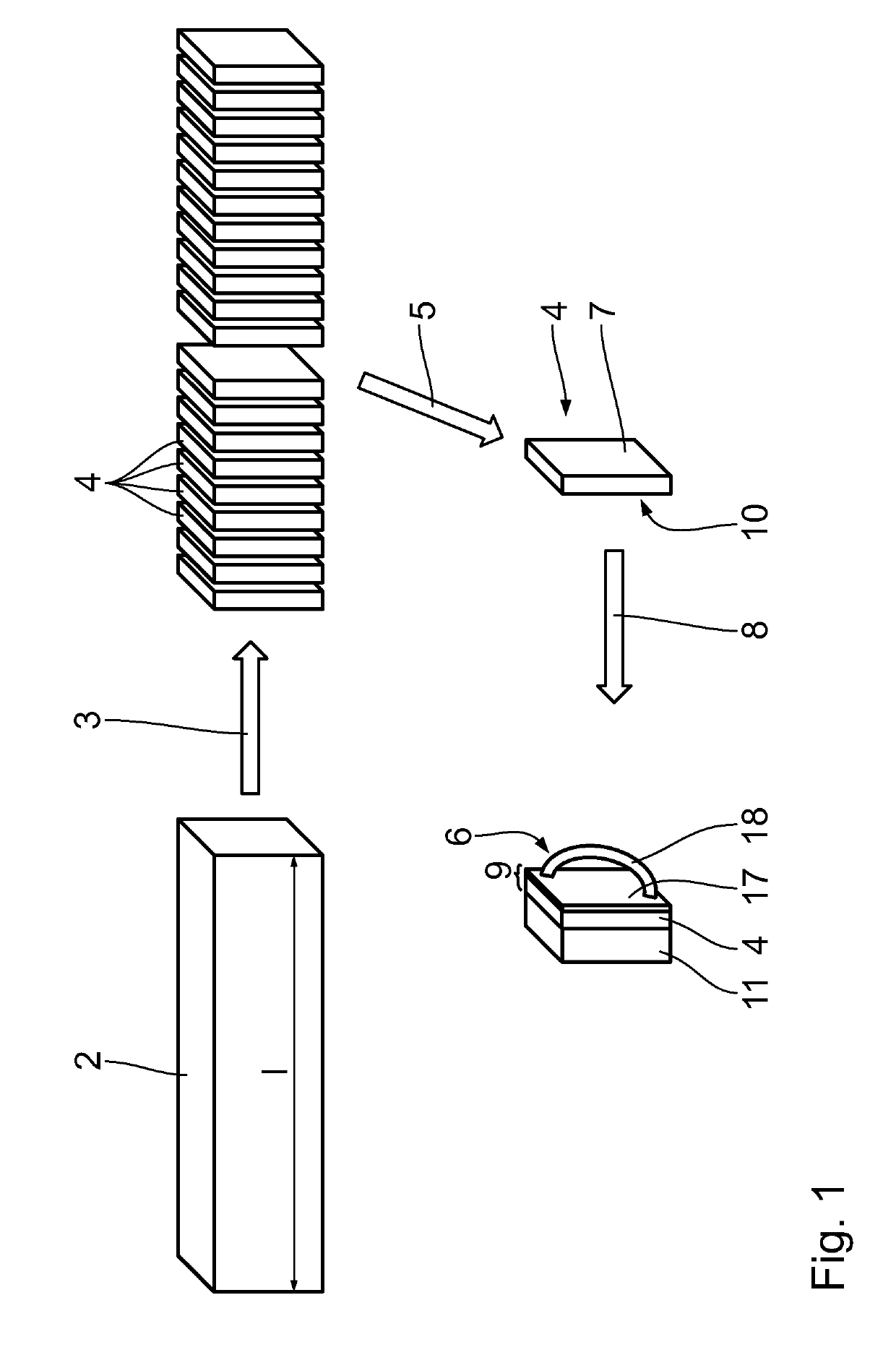
[0043]In the following method for cleaving wafers 1 is described. First a block of crystalline material, in particular a silicon block, also known as silicon ingot 2, is provided. The silicon ingot 2 can have a monocrystalline or quasi-monocrystalline structure. With the term quasi-monocrystalline a structure is denoted, which is at least in 50% of its volume, in particular at least in 70% of its volume, in particular at least in 90% of its volume monocrystalline.

[0044]The silicon ingot 2 has preferably a cylindrical or cuboid shape. It can have a length 1 of more than 20 cm, in particular more than 30 cm, in particular more than 50 cm. It can have a square or round cross section A. The cross section A can be at least 10 cm×10 cm, in particular at least 15 cm×15 cm, in particular at least 20 cm×20 cm, in particular at least 25 cm×25 cm, in particular at least 30 cm×30 cm.

[0045]In a first cutting step 3 the silicon ingot 2 is cut into slices 4. For this a wire sawing process can be u...


PUM

PropertyMeasurementUnit
thicknessaaaaaaaaaa
thicknessaaaaaaaaaa
thicknessaaaaaaaaaa

Abstract

A method for cleaving wafers comprising the following steps: providing a slice of a crystalline material with at least a first plane side, providing at least one stressing means to be attached to said slice, wherein said at least one stressing means is at least in parts made of a material with a coefficient of thermal expansion different from that of the slice, attaching said stressing means to said first plane side of said slice to form a stack, inducing a thermal shear stress to said slice by applying a temperature change to said stack.

Description

FIELD OF THE INVENTION[0001]The invention relates to a method for cleaving wafers. The invention further relates to a device for cleaving wafers.BACKGROUND OF THE INVENTION[0002]One step in the production of silicon wafers for solar cells is the separation of such wafers from silicon bricks usually done by wire saws. However, the wire sawing process leads to a rather high percentage of material loss.SUMMARY OF THE INVENTION[0003]It is an object of the invention to improve a method for the production of wafers. It is in particular an object of the invention to provide a method, which provides a significantly higher mass yield of wafers from the starting silicon block, and that the process be capable of making wafers with thicknesses from 180 microns down to 40 microns. This objective is solved by a method for cleaving wafers comprising the following steps: Providing a slice of a crystalline material with at least a first plane side, providing at least one stressing means to be attach...

Claims


Application Information

Patent Timeline
Patent Type & Authority Patents(United States)
IPC IPC(8): B26F3/00C30B33/06H01L31/18C30B29/06H01L21/67
CPCB26F3/002C30B29/06H01L31/18C30B33/06H01L21/67092Y10T225/12
Inventor STODDARD, NATHANSEIPEL, BJOERN
Owner MAXEON SOLAR PTE LTD
Why Eureka
Try Eureka