Exposure apparatus and method

a technology of exposure apparatus and udof, applied in the field of photolithographic tools, can solve the problems of reducing the useful dof (udof), reducing the depth of focus, and reducing so as to reduce the impact of the projection objective, increase the area of exposure, and increase the udof of the projection objective.

Active Publication Date: 2019-09-24
SHANGHAI MICRO ELECTRONICS EQUIP (GRP) CO LTD
View PDF14 Cites 1 Cited by
  • Summary
  • Abstract
  • Description
  • Claims
  • Application Information

AI Technical Summary

Benefits of technology

[0006]It is an objective of the present invention to provide an exposure apparatus capable of creating a field of exposure that is less affected by objective field of view (FoV) distortion and allows a higher useful depth of focus (UDoF) when compared to other fields of exposure of the same size and of creating a greater field of exposure with the same projection objective DoF.
[0024]Compared with the prior art, in the exposure apparatus and method according to the present invention, the light-homogenizing quartz rod in the light-homogenizing unit of the illumination system has a regular hexagonal cross section rather than a quadrilateral cross section, and the masks are designed as regular hexagons each matches with the cross section of the light-homogenizing quartz rod. As a result, a hexagonal field of exposure created by the cross-sectionally hexagonal light-homogenizing quartz rod has a shorter diagonal than a quadrilateral field of exposure of the same size, thereby reducing the impact of the projection objective over DoF and hence allowing a greater UDoF of the projection objective. Additionally, with the same DoF of the projection objective, a hexagonal field of exposure created by the cross-sectionally hexagonal light-homogenizing quartz rod leads to an increase in area of exposure. As the present invention allows an increased UFoV of a projection objective, it can overcome the disadvantage that defocus arising from errors occurring in focal plane control carried out by the photolithographic system may lead to a degree of inhomogeneity of a pattern image on the substrate beyond a tolerable range and can eliminate “inconsistency” or “color differences” perceivable by the naked eye. According to the present invention, the shape correspondence between the cross sections of the light-homogenizing quartz rod and the masks, as well as the design of the hexagonal masks that are put together into a whole, is particularly suitable for the imaging of dense holes or circular pillars during the fabrication of LED devices or the like. According to the present invention, the addition of the flood exposure unit and step enhance the steepness of side faces of patterns formed from the exposure process so that the patterns are more regularized in shape, which is conducive to the yield. In the exposure method according to the present invention, a tilt of each FoV with respect to an optimum focal plane can be fitted and calculated based on repeated consecutive measurements of the wafer's surface profile, followed by exposure of the wafer in one pass. Compared to the conventional approaches that involve multiple measure and exposure cycles, the sensitivity to work pieces (i.e., wafers) is reduced, and the adaptability to substrates with high hardness (e.g., sapphire substrates) or great warpage is improved. According to the present invention, exposure of the wafer in one pass entails the advantages of shorter exposure time and lower manufacturing cost.

Problems solved by technology

Compared with stripes, the imaging of dense holes or circular pillars is much more difficult and tends to suffer from a much reduced depth of focus (DoF).
On the other hand, in contrast to silicon wafers, patterned sapphire substrates are hard in nature and tend to have significant warpage, which contribute to further reductions in the useful DoF (UDoF).
With an insufficient UDoF, defocus arising from errors in the focal plane control by the photolithographic system may lead to a degree of inhomogeneity of the pattern image on the substrate that is beyond a tolerable range, which is manifested as a macro effect that portions of the pattern image on the substrate have varying degree of brightness even under the same lighting conditions, i.e., a phenomenon that “inconsistency” or “color differences” can be perceived with the naked eye.
Therefore, the control of various process parameters, especially the focal plane, is posed with highly demanding requirements.
However, the illumination system and the masks are primarily used for laser annealing, and cannot be used for the fabrication of LED devices.
The existing photolithographic tools for the exposure of patterned sapphire substrates are associated with a low yield, poor adaptability and unsuitability for mass production due to lens design cost, control system design and other reasons.

Method used


Image

  • Exposure apparatus and method
  • Exposure apparatus and method
  • Exposure apparatus and method

Examples


embodiment 1

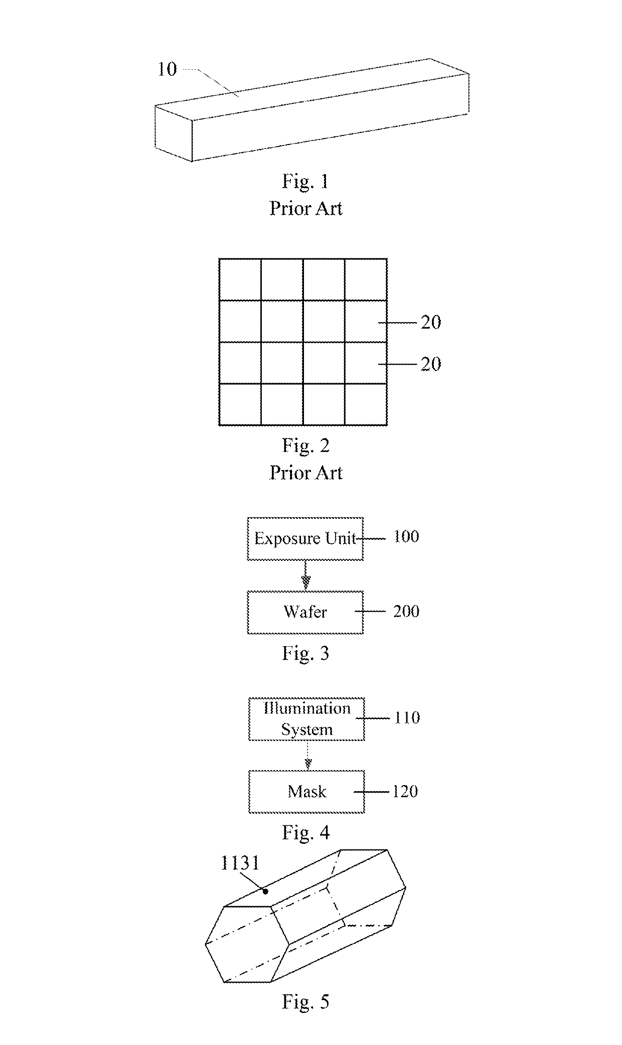
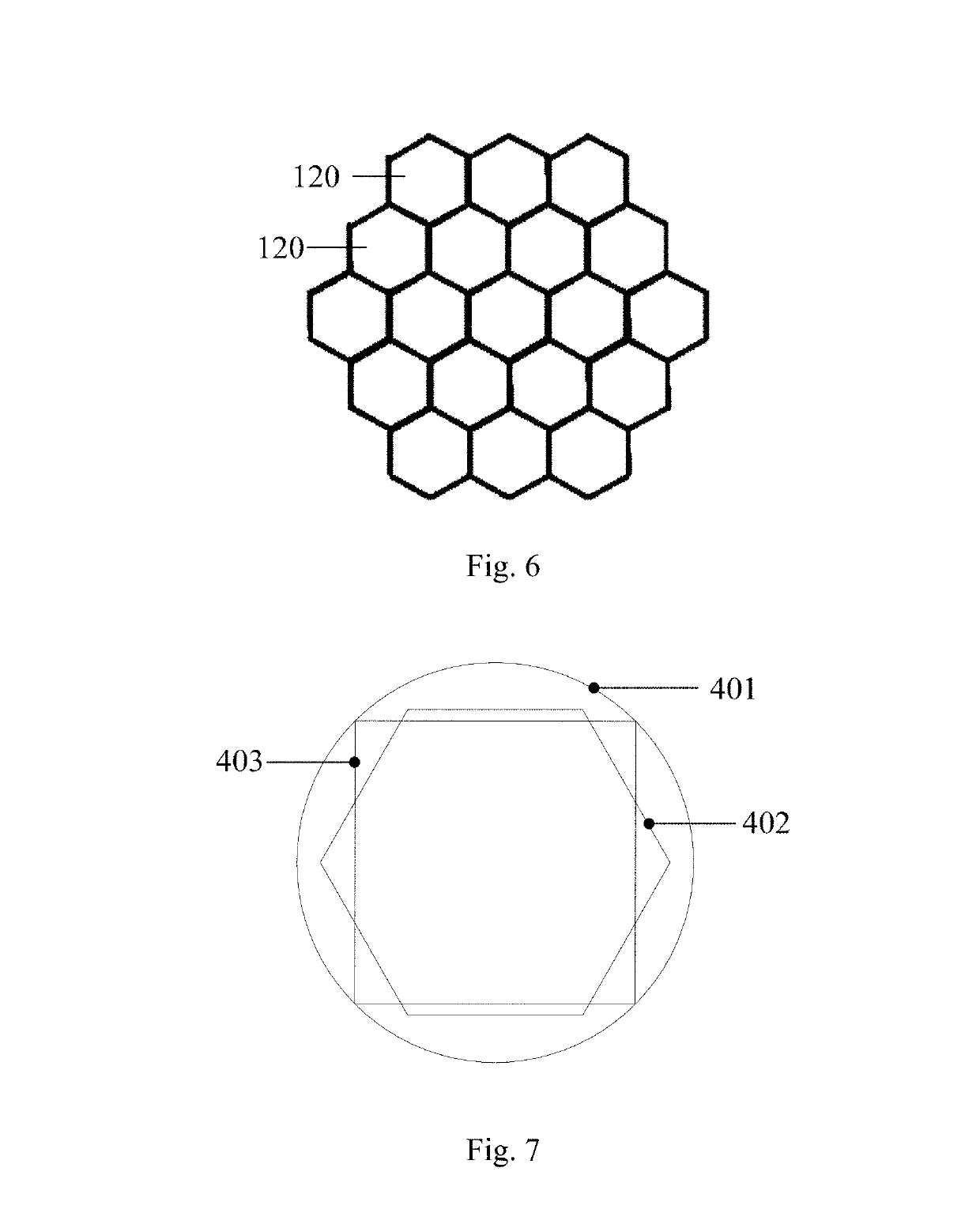
[0044]FIGS. 3 to 6 show an exposure apparatus according to a first embodiment of the present invention, including an exposure unit 100 for exposing a wafer 200. The exposure unit 100 includes an illumination system 110 and masks 120. The illumination system 110 includes a light-homogenizing unit 113. The light-homogenizing unit 113 includes a light-homogenizing quartz rod 1131 having a regular hexagonal cross section. Each mask 120 also has a regular hexagonal cross section which matches with the cross section of the light-homogenizing quartz rod 1131.

[0045]Specifically, as shown in FIG. 5, the light-homogenizing quartz rod 1131 in the light-homogenizing unit 113 of the illumination system 110 of the exposure apparatus according to the present invention has a regular hexagonal cross section rather than a quadrilateral cross section. Additionally, as shown in FIG. 6, in the exposure apparatus according to the present invention, each of the masks 120 is designed as a regular hexagon w...

embodiment 2

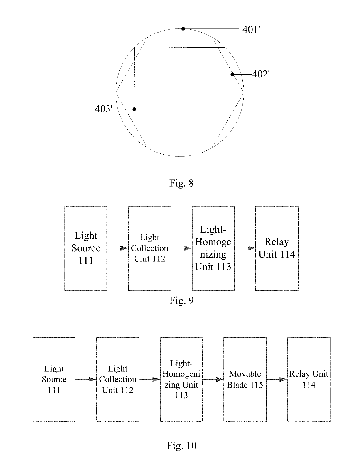
[0054]An exposure method according to a second embodiment for use with the exposure apparatus of Embodiment 1 includes at least the steps of: so designing the light-homogenizing quartz rod in the light-homogenizing unit of the illumination system that it has a regular hexagonal cross section; and so designing the masks that each of them has a shape matching with the cross section of the light-homogenizing quartz rod. A hexagonal field of exposure created by the cross-sectionally hexagonal light-homogenizing quartz rod has a shorter diagonal than a quadrilateral field of exposure of the same size, thereby reducing the impact of the projection objective over DoF and hence allowing a greater UDoF of the projection objective. Additionally, with the same DoF of the projection objective, a hexagonal field of exposure created by the cross-sectionally hexagonal light-homogenizing quartz rod is greater than a field of exposure created by a cross-sectionally quadrilateral light-homogenizing q...


PUM

PropertyMeasurementUnit
energyaaaaaaaaaa
surface profileaaaaaaaaaa
depth of focusaaaaaaaaaa

Abstract

An exposure apparatus includes an exposure unit for exposing a wafer. The exposure unit includes an illumination system and masks. The illumination system includes a light-homogenizing unit. The light-homogenizing unit includes a light-homogenizing quartz rod having a regular hexagonal cross section. Each of the masks has a regular hexagonal shape matching with the cross section of the light-homogenizing quartz rod. A field of exposure resulting from this arrangement is less affected by objective field of view distortion and allows a higher useful depth of focus (UDoF) when compared to other fields of exposure of the same size. In addition, with the same projection objective DoF, a greater field of exposure can be obtained.

Description

TECHNICAL FIELD[0001]The present invention relates to photolithographic tools and, in particular, to an exposure apparatus and method.BACKGROUND[0002]A photolithographic tool is a machine for applying a pattern onto a substrate, in particular a desired portion thereof. Such machines can be used, for example, in the fabrication of integrated circuits (ICs). In such cases, it could be considered that a pattern on a mask or reticle is used to form a pattern for a single IC layer. This pattern can be imaged onto a target site (e.g. including one or more pins) of a substrate (e.g., a silicon substrate). In particular, in the field of light-emitting diode (LED) manufacturing, a pattern of dense holes is first imaged onto a patterned sapphire substrate.[0003]Compared with stripes, the imaging of dense holes or circular pillars is much more difficult and tends to suffer from a much reduced depth of focus (DoF). Therefore, the photolithographic process is imposed with very high requirements ...

Claims


Application Information

Patent Timeline
Patent Type & Authority Patents(United States)
IPC IPC(8): G03F7/20G02B27/09H01L33/00H01L21/027H01L21/67H01L21/68
CPCG03F7/2022G03F7/2008G02B27/09H01L21/027G03F7/70075H01L21/67069H01L33/00H01L21/682G03F7/20G03F7/70641G03F7/70775G03F7/70833H01L21/673H01L21/67763
Inventor XIE, RENBIAOYANG, ZHIYONGBAI, ANGLIWANG, JIAN
Owner SHANGHAI MICRO ELECTRONICS EQUIP (GRP) CO LTD
Why Eureka
Try Eureka