Pinch-off type vertical junction field effect transistor and method of manufacturing the same

a vertical junction field and transistor technology, applied in the direction of transistors, semiconductor devices, electrical devices, etc., can solve the problem of extremely low on-resistance, achieve the effect of reducing the number of steps, avoiding the reduction of the yield due to misalignment, and reducing manufacturing costs

Inactive Publication Date: 2005-03-22
SUMITOMO ELECTRIC IND LTD
View PDF5 Cites 24 Cited by
  • Summary
  • Abstract
  • Description
  • Claims
  • Application Information

AI Technical Summary

Benefits of technology

According to this manufacturing method, etching and ion implantation can be performed using the same mask so that the number of s

Problems solved by technology

It is to be noted that there is nothing to prevent the flow of the carriers in a path leading from t

Method used


Image

  • Pinch-off type vertical junction field effect transistor and method of manufacturing the same
  • Pinch-off type vertical junction field effect transistor and method of manufacturing the same
  • Pinch-off type vertical junction field effect transistor and method of manufacturing the same

Examples


first embodiment

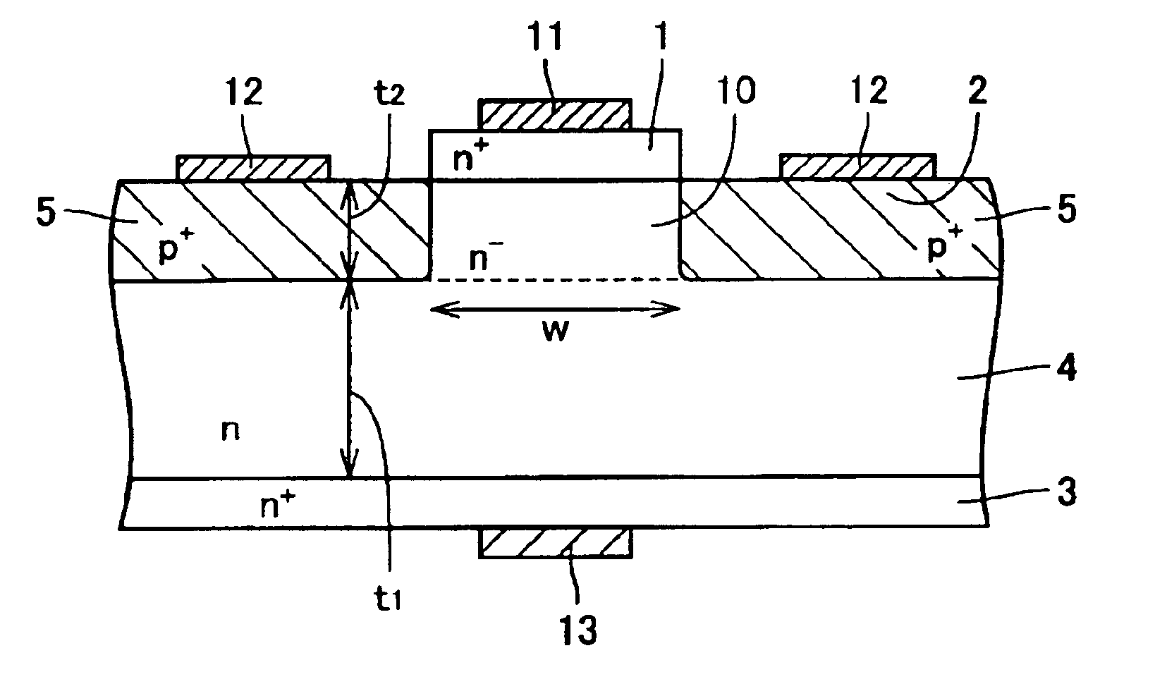
FIG. 1 is a cross sectional view of an arrangement of a JFET according to the first embodiment of the present invention. In FIG. 1, a source region 1 is formed in a shape of a projection protruding from a surface of a semiconductor substrate and includes an n type impurity of a high concentration that largely exceeds 1019 cm−3 such that an ohmic contact is established with a source electrode 11 formed by Ni, for instance. A channel region 10 includes an n type impurity at a concentration of about 1×1015 cm−3, for instance, and is formed beneath source region 1. A gate region 2 includes a p type impurity at a concentration of 1019 cm−3, for instance, and is formed on a surface immediately below each of two gate electrodes 12. A confining region 5 encloses gate region 2 and is formed to a certain thickness of the semiconductor substrate such that channel region 10 is sandwiched from either side. Confining region 5 includes the same kind of the p type impurity of the same concentration...

example corresponding to first embodiment

A semiconductor thin body and a semiconductor layer formed thereon were all formed by 4H-SiC, and withstand voltage performance and on-resistance (resistance in the on-state) of a JFET having the following dimensions were measured (with respect to a drift region thickness t1, a confining region thickness t2, a channel region width W, see FIG. 1).Drift region thickness t1,=2.2 μmConfining region thickness t2,=1 μmChannel region width W=10 μm

Result of MeasurementVoltage resistance: 380 V (gate voltage when OFF: at minus 22 V)On-resistance: 0.7 mΩ·cm2

As described above, from the FET of the present invention, a result of high withstand voltage performance and extremely low on-resistance was obtained. Consequently, since it achieves low consumed power with high withstand voltage and has a simple structure, it is easy to manufacture and the manufacturing cost can be kept low.

second embodiment

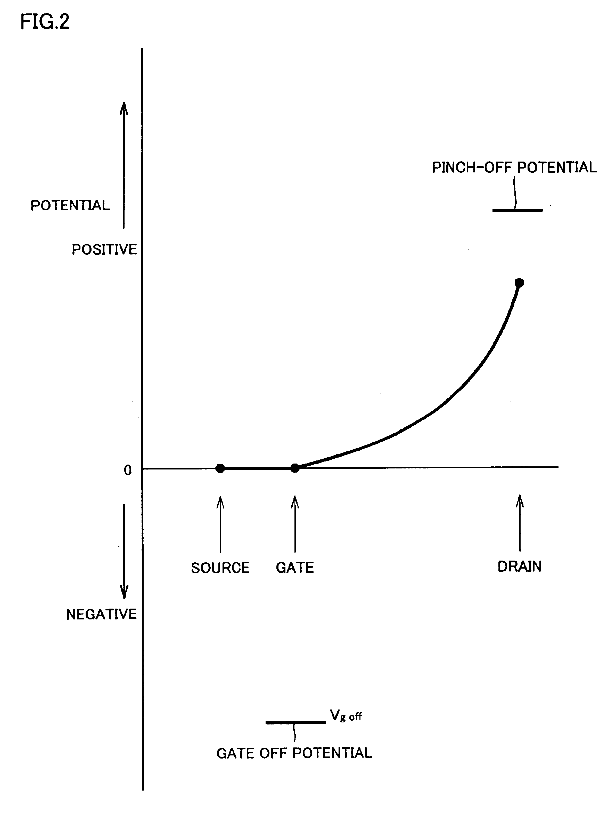
FIG. 12 is a cross sectional view of an arrangement of a JFET according to the second embodiment of the present invention. A source electrode 11 and a gate electrode 12 are provided on one main surface (front face) of a semiconductor substrate, while a drain electrode 13 is provided on the other main surface (reverse face). A source region 1 is formed in contact with source electrode 11, a gate region 2 is formed in contact with gate electrode 12, and a drain region 3 is formed in contact with drain electrode 13, respectively. Channel region 10 is provided in contact with source region 1 and gate region 2 and controls an on-state and an off-state of carriers by potentials of the gate region and the source region. To bring about the on-state, zero voltage that is the same as that applied to the source electrode or a positive voltage is applied to the gate electrode to cause the electrons of source region 1 to move toward drain region 3 having a higher potential. A drift region 4 beco...


PUM


Abstract

A junction field effect transistor (JFET) is provided that is capable of a high voltage resistance, high current switching operation, that operates with a low loss, and that has little variation. This JFET is provided with a gate region (2) of a second conductivity type provided on a surface of a semiconductor substrate, a source region (1) of a first conductivity type, a channel region (10) of the first conductivity type that adjoins the source region, a confining region (5) of the second conductivity type that adjoins the gate region and confines the channel region, a drain region (3) of the first conductivity type provided on a reverse face, and a drift region (4) of the first conductivity type that continuously lies in a direction of thickness of the substrate from a channel to a drain. A concentration of an impurity of the first conductivity type in the drift region and the channel region is lower than a concentration of an impurity of the first conductivity type in the source region and the drain region and a concentration of an impurity of the second conductivity type in the confining region.

Description

TECHNICAL FIELDThe present invention relates to a junction field effect transistor (JFET) that performs a high current, high voltage switching operation used in a direct current / alternating current conversion in power transmission and in an inverter and the like, and more specifically, to a vertical JFET that achieves further reduction in the power loss.BACKGROUND ARTA junction field effect transistor (JFET) used for switching of an inverter and the like is required to endure high current and high voltage. FIG. 25 is a diagram representing a normal horizontal JFET. In the horizontal JFET, carriers move substantially parallel to the semiconductor substrate surface. A ground potential is applied to a source region 101 through a source electrode 111, and a positive potential is applied to a drain region 103 through a drain electrode 113. A pn junction is formed below a gate region 102 beneath gate electrode 112, and when the device is caused to attain an off-state, a negative voltage i...

Claims


Application Information

Patent Timeline
IPC IPC(8): H01L21/337H01L21/02H01L29/66H01L29/772H01L29/808H01L29/24H01L29/02
CPCH01L29/0843H01L29/1058H01L29/1066H01L29/1608H01L29/8083H01L29/66909H01L29/7722H01L29/808H01L29/66901
Inventor HARADA, SHINHIROTSU, KENICHIMATSUNAMI, HIROYUKIKIMOTO, TSUNENOBU
Owner SUMITOMO ELECTRIC IND LTD
Why Eureka
Try Eureka