
Femtosecond laser-induced formation of single crystal patterned semiconductor surface

a single crystal, laser-induced technology, applied in laser beam welding apparatus, manufacturing tools, welding/soldering/cutting articles, etc., can solve the problems of significant disruption of the lattice, ultra-fast generation of point defects, and loss of efficiency within the devi

Active Publication Date: 2019-10-01
RGT UNIV OF MICHIGAN
View PDF11 Cites 0 Cited by
  • Summary
  • Abstract
  • Description
  • Claims
  • Application Information

AI Technical Summary

Benefits of technology

[0007]Accordingly, the teachings of the present invention are applicable to a wide range of devices including but not limited to solar cells, batteries, chemical, biological, light sensors, and the like. The ability to process in air makes this novel approach even more attractive for producing a product. Furthermore, this process is easily combined with traditional manufacturing methods for these kinds of devices such as, but not limited to, molecular beam expitaxy, chemical beam expitaxy, gas entrainment deposition, atomic layer deposition, and sputter deposition. Such combinations, along with thermal annealing techniques, greatly enhance our claims as we can produce pn junctions, Schottky or Ohmic contacts, modulation doped layers, etc. to create novel devices.
[0024]LSFL can form on a smooth surface with as few as two exposures. The first exposure ablates material creating features, such as crater edges, on the surface. On the second exposure, LSFL form when ultrashort laser pulses interact with a roughened semiconductor surface. Excitation generates a dense electron-hole plasma driving the real part of the semiconductor's dielectric function negative, which allows light to couple to plasmons to form surface plasmon polaritons (SPPs). The surface features formed on the first laser exposure allow the light to interact with parts of the surface at a nonzero angle, which provides the necessary component of momentum in the surface direction, perpendicular to the laser polarization, for the photons to excite SPPs. The LSFL form with their long axis perpendicular to the laser polarization via selective ablation where the SPP is locally most intense. The LSFL initially form at ASPP, which varies depending on the plasma density. On subsequent laser exposures, the SPPs can couple to the pre-existing LSFL at a grating coupled wavelength shorter than ASPP. When SPPs interact with a pre-existing grating, they Bragg scatter, which leads to a decrease in the grating coupled wavelength as more material is removed after each pulse until it reaches a minimum at λSPP / 2.
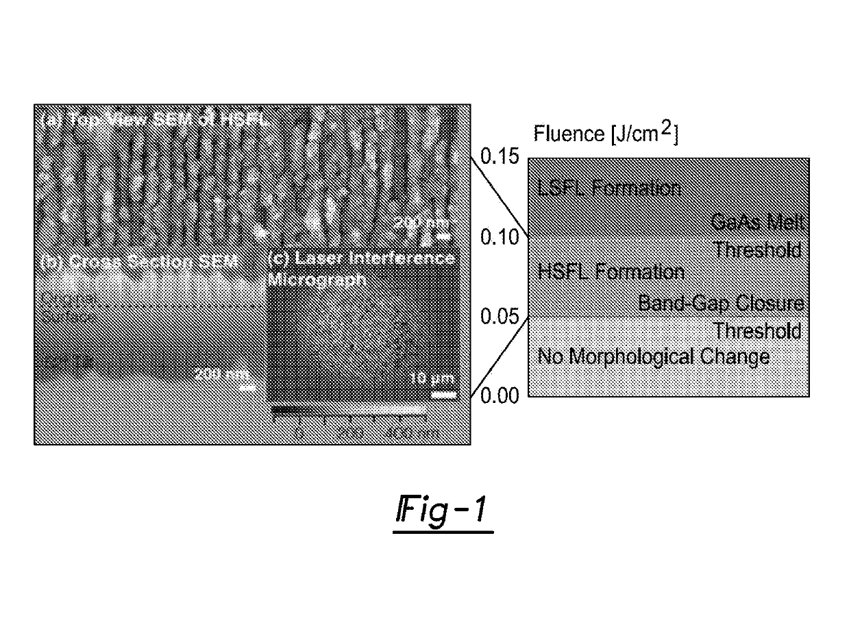
[0043]Experiments performed on InSb and also previous simulations on GaAs, Si, and InSb reveal that during or immediately after a sufficiently intense laser pulse the average ion motion is essentially freely drifting due to the weakening of the attractive part of the interatomic potential that results from the excitation of valence-band electrons to conduction-band states. FIG. 7 shows the average atomic displacements of the Ga cations and the As anions from the ideal 0° K positions for fluence 0.199 J / cm2, 81.6% of the simulated band-gap closure threshold, and 0.244 J / cm2—the simulated band-gap closure threshold in a and b respectively. The model fluences are above the experimental values due to an underestimation of the dielectric function in the model. The displacement is characterized by an initial rapid increase of the average displacement for ≈200 fs after the laser pulse followed by the establishment of a new mean distance even though the temperature has only slightly increased, as shown in FIG. 8. The relatively small ion temperature increases in the midst of such large atomic displacements is indicative of both the nonthermal and ultrafast nature of the point defect formation mechanism. Also shown in FIG. 7(a) is the motion of one particular As anion that showed large displacement from the mean within 1 ps of the laser pulse. This is the lowest fluence at which such large displacements were observed. The large excursion of this atom from the mean appears to be due to its initial position close to its 0° K equilibrium site along with momentum away from this site at the onset of the laser pulse. It is at this fluence that it is suspected that defect formation is initiated, although one should be cautious in placing too much significance on individual trajectories in mean-field simulations. At the band-gap closure threshold of 0.244 J / cm2, 14.2% of the valence electrons are excited. In this case, the average cation and anion displacements have increased substantially in FIG. 7(b). At this fluence, diffusive behavior is seen as characterized by the gradually increasing displacement that begins at ≈800 fs. Under these conditions, some fraction of the ions will drift more than an Å, and those with favorable initial conditions can reach an interstitial site. The interstitial site represents the real space location with the highest density of excited electrons after irradiation, and thus represents a likely site for excited electrons to recombine with an ion core. A configurational change that forms a vacancy / interstitial pair, similar to a dissociated Frenkel Pair, serves as a non-radiative pathway for the electrons to reoccupy bonding states. Repeating this process over multiple exposures causes defects to accumulate as long as the generation rate exceeds the recombination rate. The experimental and modeling evidence indicates that this threshold is the same as that for band-gap closure. The softened binding potential also increases mobility for previously generated defects. This both increases the probability of vacancy / interstitial pair dissociation and may enhance diffusivity of the resulting vacancies and self-interstitials.
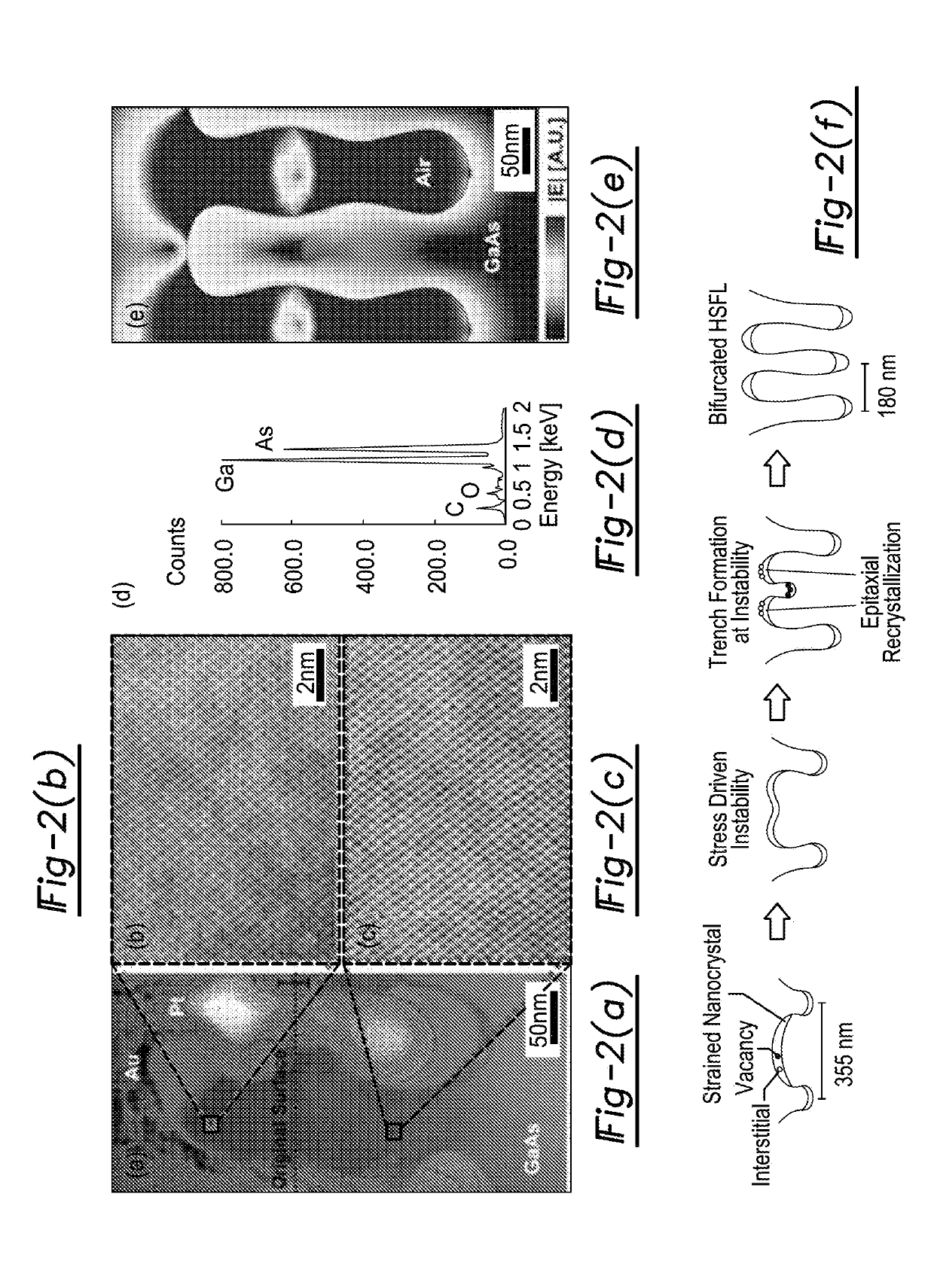
[0049]where λ is the stable wavelength, M is the modulus, γ is the surface energy, and σ is the stress. For the ground state InGaAs / GaAs, ≈0.5 J / m2 and M is 147 GPa. This yields a bifurcation stress of 1.3 GPa. This value is consistent with the 1-5 GPa that build up in the near surface from vacancies / interstitial generation during ion beam growth of ripples. The vacancy rich nanocrystalline region also increases mobility during recrystallization, growing a single crystal above the original surface, shown in cross-section STEM in FIG. 2(b), that remains epitaxial to the GaAs below the original surface in FIG. 2(c). The recrystallization process provides an alternate vacancy sink, which prevents the material from accumulating sufficient stress to drive a second LIPSS bifurcation. The combination of interstitial and vacancy diffusion produces HSFL with an amplitude of 350-400 nm after 1,500 exposures in FIG. 2(a) that retain their original stoichiometry in cross-section STEM energy dispersive x-ray spectroscopy in FIG. 2(d). A schematic of this stress-driven bifurcation mechanism is provided in FIG. 2(f). Further, Ga droplets are not observed on the structure surfaces, which indicates that growth temperature does not exceed 933° K and is consistent with ion temperatures during defect formation predicted by QMD in FIG. 8.
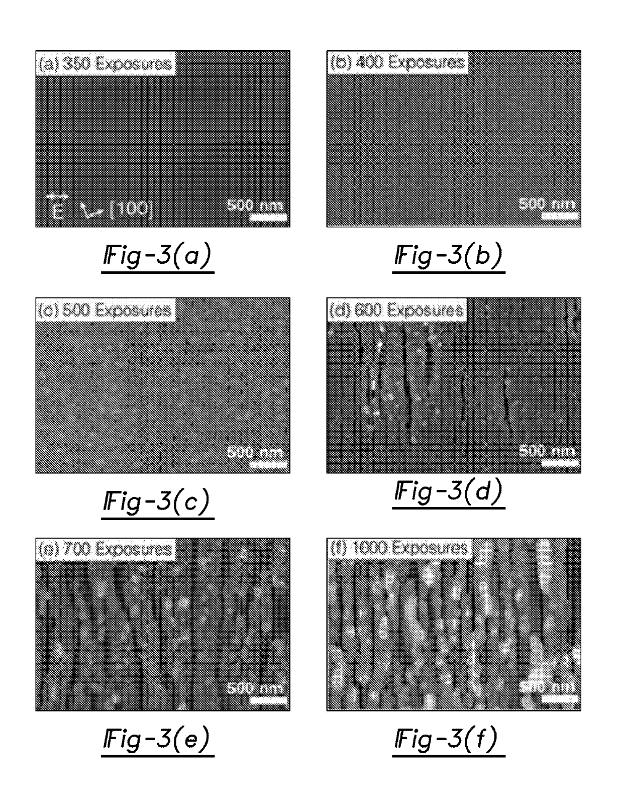
[0053]2. The combination of growth from the bulk generated interstitials and surface coarsening leads to larger random but fewer islands that are also spaced further apart.
[0062]This process can occur in ambient condition (in air) without the need for a high vacuum system. This is a remarkable finding in itself because it has been commonly believed that epitaxial redistribution near a surface requires a vacuum. Hence, the present teachings are applicable to a wide range of devices including, but not limited to, solar cells, batteries, chemical, biological, and light sensors etc. The ability to process in air makes this novel approach even more attractive for producing a product. Furthermore, this process is easily combined with traditional manufacturing methods for these kinds of devices such as, but not limited to, molecular beam expitaxy, chemical beam expitaxy, gas entrainment deposition, atomic layer deposition, and sputter deposition. Such combinations, along with thermal annealing techniques, greatly enhance the benefits of the present teachings by enabling production of pn junctions, Schottky or Ohmic contacts, modulation doped layers, etc. to create novel devices.

Problems solved by technology

Many surface patterning techniques do not retain the semiconductor's original crystal structure, which leads to efficiency losses within devices.
The reason for this is that either ablation or at least melting occurs in all of these techniques, which leads to significant disruption of the lattice.
HSFL formation is initiated when the intense laser field softens the interatomic binding potential, which leads to an ultrafast generation of point defects.

Method used


Image

  • Femtosecond laser-induced formation of single crystal patterned semiconductor surface
  • Femtosecond laser-induced formation of single crystal patterned semiconductor surface
  • Femtosecond laser-induced formation of single crystal patterned semiconductor surface

Examples


Embodiment Construction

[0021]Example embodiments will now be described more fully with reference to the accompanying drawings. Example embodiments are provided so that this disclosure will be thorough, and will fully convey the scope to those who are skilled in the art. Numerous specific details are set forth such as examples of specific components, devices, and methods, to provide a thorough understanding of embodiments of the present disclosure. It will be apparent to those skilled in the art that specific details need not be employed, that example embodiments may be embodied in many different forms and that neither should be construed to limit the scope of the disclosure. In some example embodiments, well-known processes, well-known device structures, and well-known technologies are not described in detail.

[0022]The terminology used herein is for the purpose of describing particular example embodiments only and is not intended to be limiting. As used herein, the singular forms “a,”“an,” and “the” may b...


PUM

PropertyMeasurementUnit
heightaaaaaaaaaa
diameteraaaaaaaaaa
diameteraaaaaaaaaa

Abstract

The interaction between multiple intense ultrashort laser pulses and solids typically produces a regular nanoscale surface corrugation. A coupled mechanism has been identified that operates in a specific range of fluences in GaAs that exhibits transient loss of the imaginary part of the dielectric function and X2, which produces a unique corrugation known as high spatial frequency laser induced periodic surface structures (HSFL). This mechanism is unique in that the corrugation does not involve melting or ablation.

Description

CROSS REFERENCE TO RELATED APPLICATIONS[0001]This application is a U.S. National Phase Application under 35 U.S.C. 371 of International Application No. PCT / US2016 / 052212 filed on Sep. 16, 2016 and published in English as WO 2017 / 053198 A2 on Mar. 30, 2017. This application claims the benefit of U.S. Provisional Application No. 62 / 219,805, filed on Sep. 17, 2015. The entire disclosures of the above applications are incorporated herein by reference.GOVERNMENT INTEREST[0002]This invention was made with government support under FA9550-12-1-0465 awarded by the Air Force Office of Scientific Research. The Government has certain rights in the invention.FIELD[0003]The present disclosure generally relates to methods of processing semiconductor surfaces by modifying the surface topography and, more particularly, relates to femtosecond laser-induced formation of a single crystal patterned semiconductor surface without melting or ablation.BACKGROUND AND SUMMARY[0004]This section provides backgr...

Claims


Application Information

Patent Timeline
Patent Type & Authority Patents(United States)
IPC IPC(8): B23K26/53B23K26/0622H01L21/02B23K103/00
CPCB23K26/53B23K26/0624H01L21/02686H01L21/02546H01L21/02549H01L21/02587H01L21/02521B23K2103/56
Inventor ABERE, MICHAEL J.YALISOVE, STEVENTORRALVA, BEN
Owner RGT UNIV OF MICHIGAN
Learn More