Method for polishing silicon wafer

a technology of silicon wafer and polishing method, which is applied in the direction of grinding/polishing apparatus, manufacturing tools, lapping machines, etc., can solve the problems of reducing the characteristics of a semiconductor device formed by the wafer, affecting the polishing rate, so as to and reduce the occurrence of impurity contamination

Active Publication Date: 2019-10-29
SHIN-ETSU HANDOTAI CO LTD
View PDF29 Cites 0 Cited by
  • Summary
  • Abstract
  • Description
  • Claims
  • Application Information

AI Technical Summary

Benefits of technology

[0033]The method for polishing a silicon wafer of the present invention can reduce the occurrence of impurity contamination due to the polishing abrasive grains since unused polishing abrasive grains are not added to the used slurry. Moreover, adding the mixed alkali solution containing a chelating agent into the recovered used slurry allows the chelating agent in the used slurry to be kept at an appropriate amount, highly maintaining the trapping effect of the chelating agent on metal impurities. Furthermore, since the mixed alkali solution contains either or both of a pH adjuster and a polishing rate accelerator, adding the mixed alkali solution into the used slurry allows adjustment of the polishing rate. Thus, a desired polishing rate can be achieved. In addition, since additional polishing abrasive grains are not supplied and the metal impurity contamination is reduced, the consumption of the polishing abrasive grains and the chelating agent can be reduced, and the silicon wafer can be polished at low cost.

Problems solved by technology

In particular, metal impurities such as copper and nickel in the silica abrasive grains, which have lower ionization tendency than hydrogen, dissolve as metal ions in the alkali slurry, precipitate on the wafer surface during polishing of the silicon wafer, and deeply diffuse into silicon inside, thus degrading wafer quality and significantly lowering characteristics of a semiconductor device formed by the wafer.
However, it is difficult to completely remove metal impurities in the silica abrasive grains.
Therefore, there is a risk of increasing metal impurities unless the polishing abrasive grains and the water-soluble chelating agent are simultaneously supplied at a constant concentration ratio.
However, since the alkali amine has high silicon etching rate, a remaining amine can locally etch the surface of the silicon wafer after completion of polishing, causing local roughness.
This yields inferior products.

Method used


Image

  • Method for polishing silicon wafer
  • Method for polishing silicon wafer
  • Method for polishing silicon wafer

Examples


example

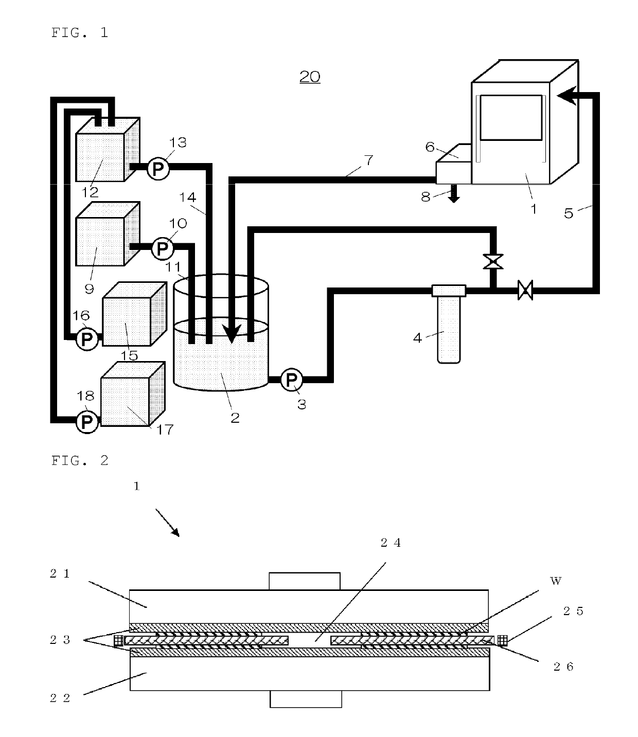
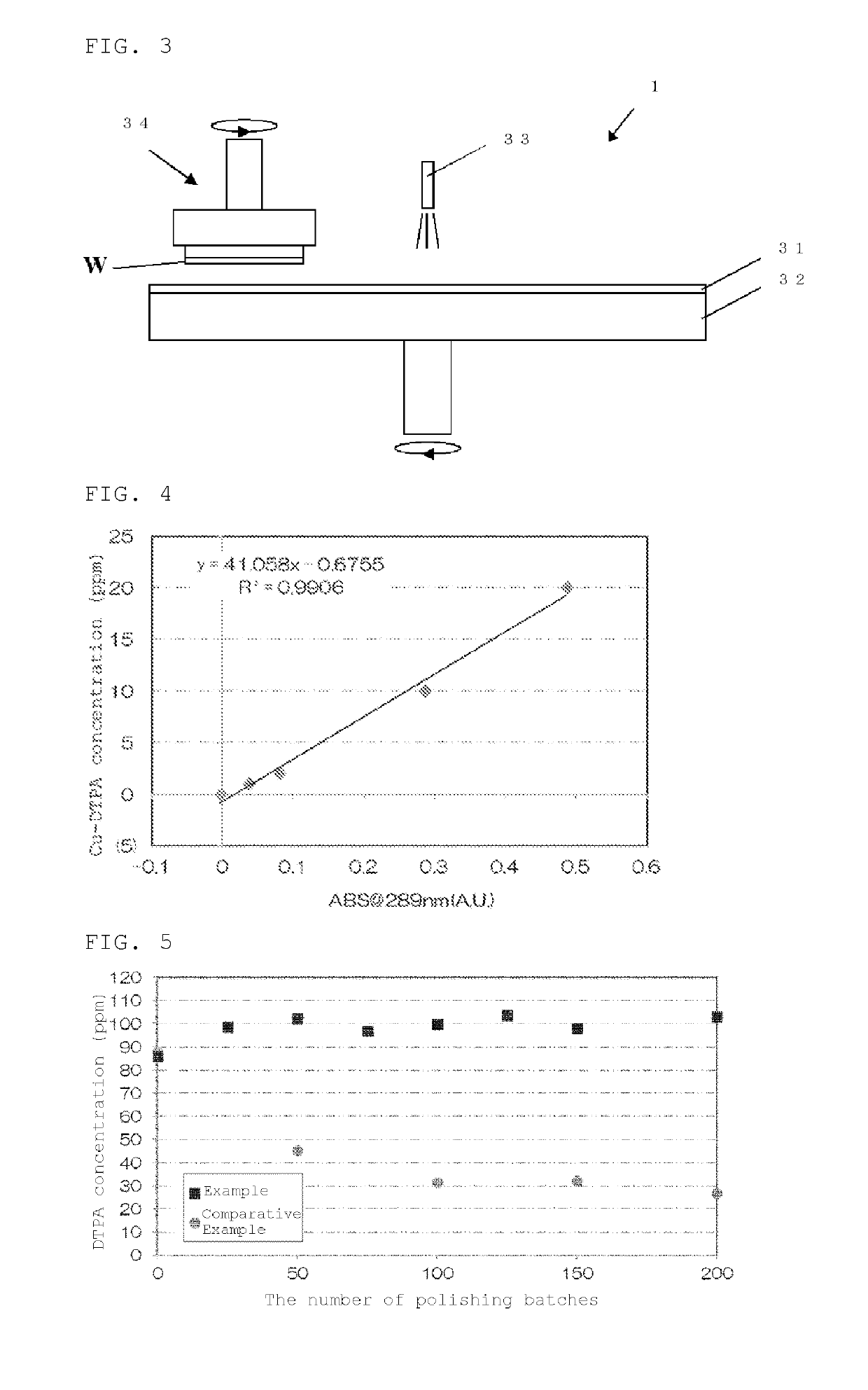
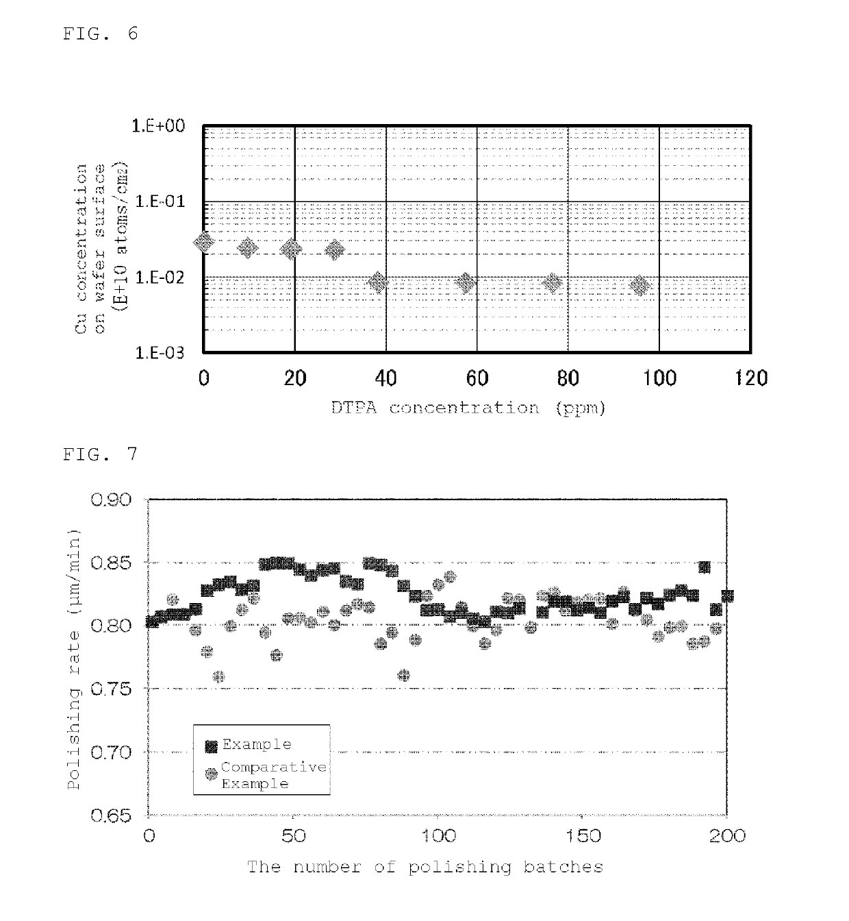
[0072]Both surfaces of silicon wafers were polished by a slurry recycling system 20 as shown in FIG. 1, according to the method for polishing a silicon wafer of the present invention. In this example, a 20B double-side polishing apparatus manufactured by Fujikoshi Machinery Corp., was used as the polishing apparatus 1. A urethane foam pad was used as the polishing pad, and 200 g / cm2 of surface pressure was applied to the silicon wafer during polishing. The polishing amount was 20 μm in total of both surfaces. Under such polishing conditions, five silicon wafers with a diameter of 300 mm were polished in one batch, and 200 polishing batches were successively carried out.

[0073]The initial slurry was created in the following manner. First, commercially available high-purified colloidal silica with a primary particle size of 0.035 μm (silica concentration: 20 mass %) was prepared in the polishing abrasive grain supplying tank 9, and diluted with pure water in the slurry supplying tank 2...


PUM

PropertyMeasurementUnit
diameteraaaaaaaaaa
thicknessaaaaaaaaaa
diameteraaaaaaaaaa

Abstract

The present invention is method for polishing silicon wafer, the method including recovering used slurry containing polishing abrasive grains that have been supplied to the silicon wafer and used for polishing, and circulating and supplying the recovered used slurry to the silicon wafer to polish the silicon wafer, wherein mixed alkali solution containing chelating agent and either or both of a pH adjuster and a polishing rate accelerator is added to the recovered used slurry without adding unused polishing abrasive grains, and the recovered used slurry is circulated and supplied to the silicon wafer to polish the silicon wafer. As a result, there is provided a method for polishing a silicon wafer that can suppress the occurrence of metal impurity contamination and stabilize the composition (e.g., the concentration of the chelating agent) of the used slurry when the used slurry is circulated and supplied to the silicon wafer for polishing.

Description

TECHNICAL FIELD[0001]The present invention relates to a polishing process for processing a silicon wafer with a polishing slurry.BACKGROUND ART[0002]In general, a silicon wafer (hereinafter, also simply referred to as a wafer) with a diameter of 300 mm or more is produced through the following producing processes. First, a silicon ingot is sliced into thin disk-shaped silicon wafers in a slicing process, and the outer region of the wafer obtained in the slicing process is chamfered in a chamfering process to prevent a fracture and a chip in the wafer. Then, the chamfered wafer is flattened in a lapping process, and mechanical damage remaining in the chamfered and lapped wafer is removed in an etching process. Then, the surface of the etched wafer is mirror-polished and flattened in a polishing process, and the polished wafer is cleaned in a cleaning process to remove a polishing slurry and foreign substances attached to the wafer.[0003]The processes described above are only main pro...

Claims


Application Information

Patent Timeline
Patent Type & Authority Patents(United States)
IPC IPC(8): H01L21/304B24B55/12B24B37/04B24B37/005B24B57/02
CPCB24B55/12H01L21/304B24B37/0056B24B57/02B24B37/04H01L21/02013
Inventor SASAKI, MASANAOHASHIMOTO, HIROMASAFUJIYAMA, KEI
Owner SHIN-ETSU HANDOTAI CO LTD
Why Eureka
Try Eureka