All optical fast fourier transform on chip with heating tunability design, simulation, fabrication, and performance analysis

a technology of fourier transform and heating tunability, applied in the field of optical fast fourier transform (offt) on chip design, to achieve the effect of simplifying circuit complexity, maximizing data rate per operation, and minimizing footprint and energy of such operations

Active Publication Date: 2019-11-19
GEORGE WASHINGTON UNIVERSITY
View PDF5 Cites 3 Cited by
  • Summary
  • Abstract
  • Description
  • Claims
  • Application Information

AI Technical Summary

Benefits of technology

[0010]The invention integrates the Optical Fast Fourier Transform (OFFT) on-chip (i.e., an integrated circuit—on a photonic wafer (such as silicon, SiN, or SiO2) semiconductor chip) to minimize the footprint and energy of such operations and maximize the data rate per operation, which is a significant step forward in communication and computation. These constraints of Hillerkus can be bypassed by implementation of all optical devices on-chip. For scaling convenience, this invention utilizes the concept of a simplified FFT scheme proposed by Hillerkuss et al. to simplify the circuit complexity. This, however, is not a necessity, but helps to keep the footprint low. Simplified OFFT has advantages such as higher speed (i.e. short delay), and less energy consumption. This is done by reordering the delays and relabeling the outputs accordingly where a simpler implementation can be found for the optical circuit since the typical FFT algorithm (decimation in time) would be difficult to implement due to its frequent waveguide crossings and large number of waveguide phases that must be accurately controlled. See Hillerkuss 3.
[0011]The present invention explores the on-chip characteristics of the OFFT for the first time and investigates how the change in design affects the quality of the output as a function of phase, time delay, and optical loss. We aim to reduce the power consumption, and a boost in data-handling capability at the same time, while minimizing crosstalk from RF signal-coupling, temperature and other external factors that can couple into the prior-art (i.e. fiber-based).

Problems solved by technology

This is done by reordering the delays and relabeling the outputs accordingly where a simpler implementation can be found for the optical circuit since the typical FFT algorithm (decimation in time) would be difficult to implement due to its frequent waveguide crossings and large number of waveguide phases that must be accurately controlled.
Also, this design is benign with hetero integration strategies.

Method used


Image

  • All optical fast fourier transform on chip with heating tunability design, simulation, fabrication, and performance analysis
  • All optical fast fourier transform on chip with heating tunability design, simulation, fabrication, and performance analysis
  • All optical fast fourier transform on chip with heating tunability design, simulation, fabrication, and performance analysis

Examples


Embodiment Construction

[0041]In describing the illustrative, non-limiting preferred embodiments of the invention illustrated in the drawings, specific terminology will be resorted to for the sake of clarity. However, the invention is not intended to be limited to the specific terms so selected, and it is to be understood that each specific term includes all technical equivalents that operate in similar manner to accomplish a similar purpose. Several preferred embodiments of the invention are described for illustrative purposes, it being understood that the invention may be embodied in other forms not specifically shown in the drawings.

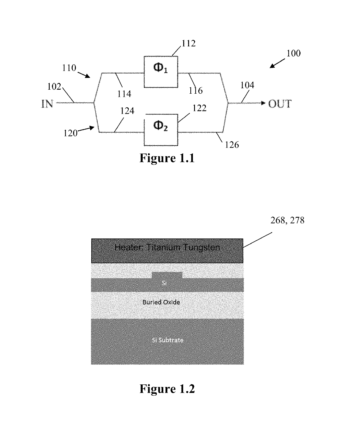
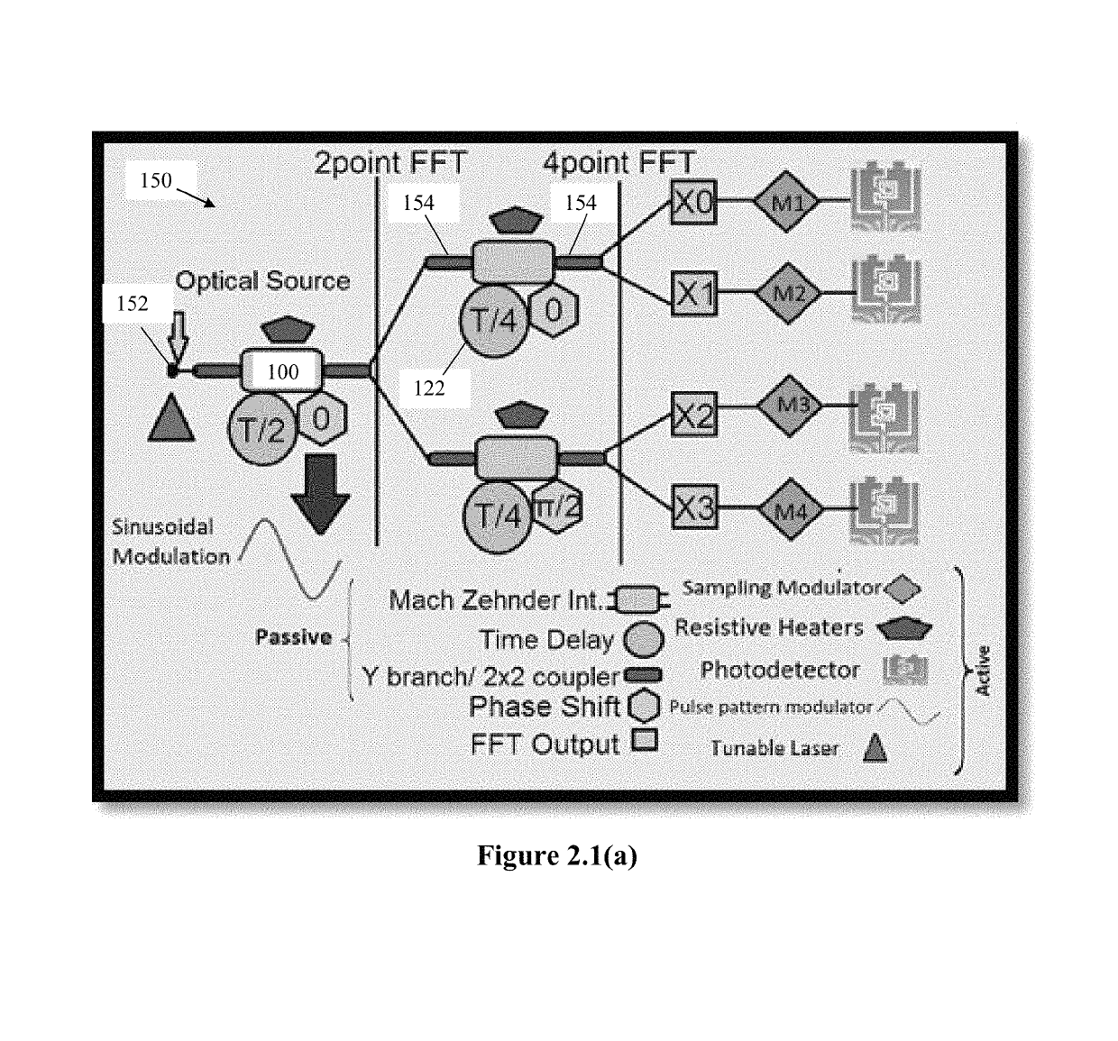
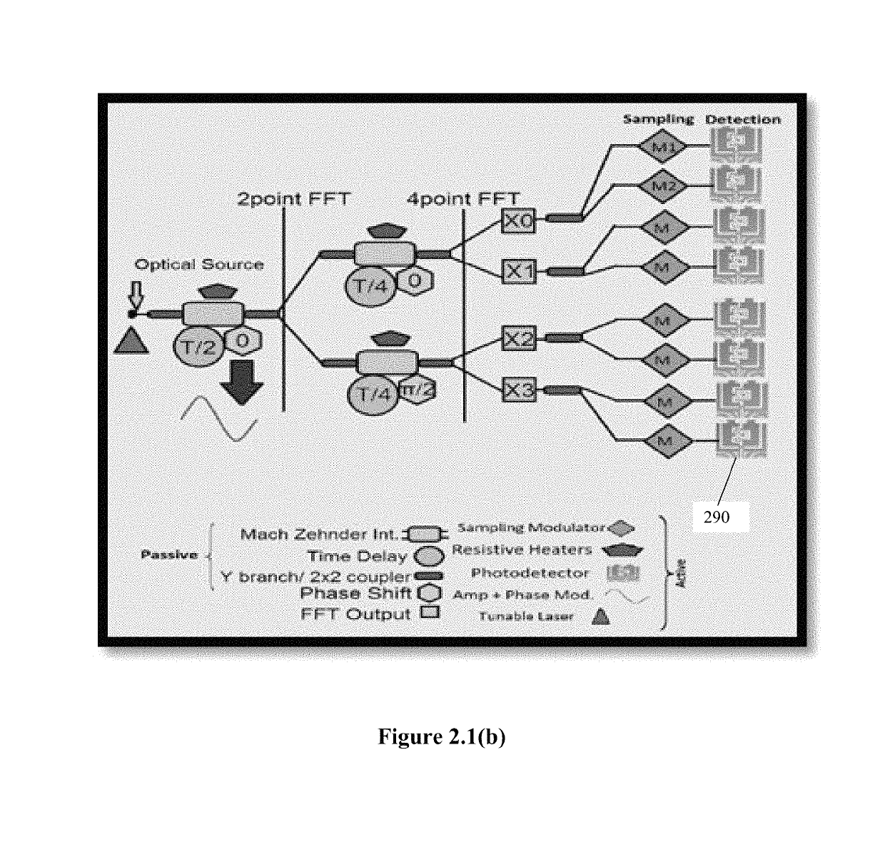
The Optical FFT (OFFT) Design

[0042]One of the earliest uses for optics in computing was frequency domain filtering with Fourier Optics. In these systems, a lens is used to convert an image into the frequency domain where filtering can occur with the result being converted back into the spatial domain with a second lens. Even though such systems are highly parallel, they are ...


PUM

PropertyMeasurementUnit
insertion lossaaaaaaaaaa

Abstract

The present invention provides optical computing by means of fast Fourier transform Integration on Silicon On Insulator chip technology with implementation in the analog and temporal domain. This is done by cascading (N−2) stages of delayed interferometers (couplers and phase shifters) where a parallel set of N time samples are taken and using the delay lines and phase of the optical components (constructive / deconstructive interference) the DFT is computed. The Optical Fast Fourier Transform (OFFT) design was built on passive components (2×2 couplers: cascaded Mach Zehnder Interferometer) used for addition and subtraction through optical interference, waveguides with short path differences are used for phase shifting and waveguides with long path differences are used for signal delay based on the needed number of outputs. Since the OFFT is a system of imbalanced interferometers, there are additional bends designed to compensate for the difference in power ratios of the arms.

Description

RELATED APPLICATIONS[0001]This application claims the benefit of U.S. Provisional Application No. 62 / 555,531, filed Sep. 7, 2017, the entire contents of which are incorporated herein by reference.BACKGROUND OF THE INVENTION[0002]Field of the Invention[0003]The present invention relates to Optical Fast Fourier Transform (OFFT) On Chip design.[0004]Background of the Related Art[0005]Fast Fourier Transform (FFT) has a widespread usage in data and single processing applications such as convolutions, filtering, image processing and data-communication. For instance, the functional analysis of convolution has widespread applications in numerical linear algebra, computer vision, language- image- and signal processing, and neural networks. Discrete convolution is defined for functions on the set of integers, which can be represented with the residue number system (RNS). Conceptually, RNS enables dimensionality reduction of an arithmetic problem by representing a large number as a set of smal...

Claims


Application Information

Patent Timeline
Patent Type & Authority Patents(United States)
IPC IPC(8): G02F1/035G02F1/01G06E3/00G02F1/225G02F1/21
CPCG02F1/225G06E3/003G02F1/0147G02F2001/215G02F2001/212G02F1/212G02F1/215
Inventor NEJADRIAHI, HANISORGER, VOLKER J.
Owner GEORGE WASHINGTON UNIVERSITY
Why Eureka
Try Eureka