Semiconductor device manufacturing method with reduced gate electrode height loss and related devices

a technology of semiconductor devices and manufacturing methods, applied in the field of semiconductor devices, can solve problems such as the peeling of the electrodes, and achieve the effect of reducing the loss of the interlayer dielectric layer and reducing the height loss of the gate electrodes

Active Publication Date: 2020-01-14
SEMICONDUCTOR MANUFACTURING INTERNATIONAL (BEIJING) CORP +1
View PDF10 Cites 0 Cited by
  • Summary
  • Abstract
  • Description
  • Claims
  • Application Information

AI Technical Summary

Benefits of technology

[0013]This inventive concept presents both a semiconductor device and its manufacturing method. The inventive concept disclosed herein can reduce the loss of the interlayer dielectric layer in the manufacturing process and therefore reduce the height loss of the gate electrode.

Problems solved by technology

In actual manufacturing process, a structure with too large H1 may block the ion implantation process or cause the pseudo gate electrode to peel off; while a structure with too small H2 may have a homogeneous issue as a result of drifts or variations in the heights of different devices.
For example, when H2 is too small, metal contact components may only contact the metal gate electrodes in some devices, but not in other devices.

Method used


Image

  • Semiconductor device manufacturing method with reduced gate electrode height loss and related devices
  • Semiconductor device manufacturing method with reduced gate electrode height loss and related devices
  • Semiconductor device manufacturing method with reduced gate electrode height loss and related devices

Examples


Embodiment Construction

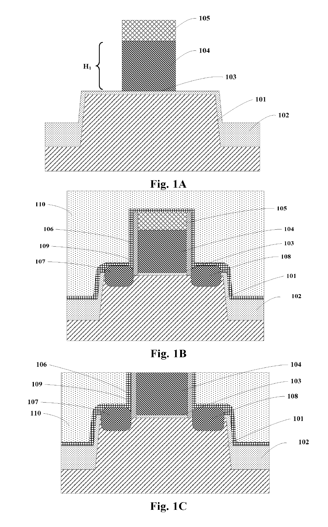
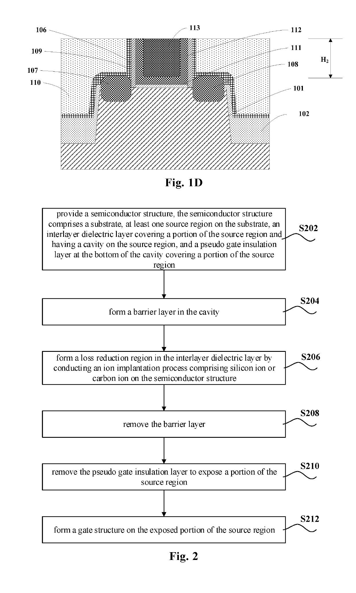
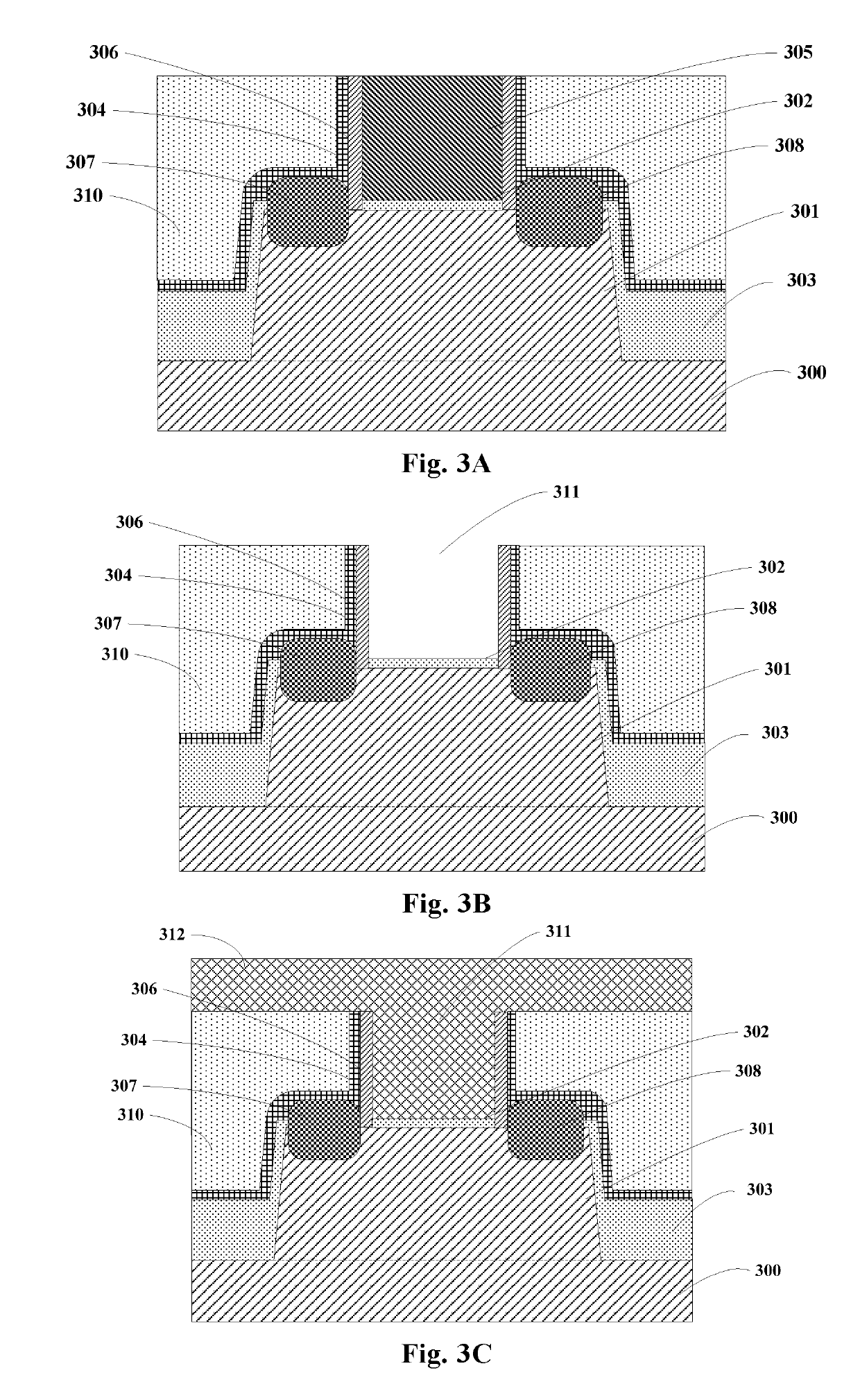
[0126]Example embodiments of the inventive concept are described with reference to the accompanying drawings. As those skilled in the art would realize, the described embodiments may be modified in various ways without departing from the spirit or scope of the inventive concept. Embodiments may be practiced without some or all of these specified details. Well known process steps and / or structures may not be described in detail, in the interest of clarity.

[0127]The drawings and descriptions are illustrative and not restrictive. Like reference numerals may designate like (e.g., analogous or identical) elements in the specification. To the extent possible, any repetitive description will be minimized.

[0128]Relative sizes and thicknesses of elements shown in the drawings are chosen to facilitate description and understanding, without limiting the inventive concept. In the drawings, the thicknesses of some layers, films, panels, regions, etc., may be exaggerated for clarity.

[0129]Embodim...


PUM

PropertyMeasurementUnit
temperatureaaaaaaaaaa
semiconductor structureaaaaaaaaaa
semiconductoraaaaaaaaaa

Abstract

A semiconductor device and its manufacturing method are presented. The manufacturing method includes providing a semiconductor structure comprising a substrate, at least one source region on the substrate, an interlayer dielectric layer covering a portion of the source region and having a cavity on the source region, and a pseudo gate insulation layer at the bottom of the cavity covering a portion of the source region; forming a barrier layer in the cavity; forming a loss reduction region in the interlayer dielectric layer by conducting an ion implantation process comprising silicon ion or carbon ion; removing the barrier layer; removing the pseudo gate insulation layer to expose a portion of the source region; and forming a gate structure on the exposed portion of the source region. This inventive concept reduces the loss of the interlayer dielectric layer, thus reduces the height loss of the gate electrode.

Description

CROSS-REFERENCE TO RELATED APPLICATION[0001]This application claims priority to and benefit of Chinese Patent Application No. 201611066969.4 filed on Nov. 29, 2016, which is incorporated herein by reference in its entirety.BACKGROUND(a) Field of the Invention[0002]This inventive concept relates to semiconductor technology and, more specifically, to a semiconductor device and its manufacturing method.(b) Description of the Related Art[0003]In conventional Metal Oxide Semiconductor Field Effect Transistor (MOSFET) manufacturing processes, a gate electrode is typically manufactured by a gate-last process, which is described below with reference to FIGS. 1A, 1B, 1C, and 1D.[0004]Referring to FIG. 1A, a semiconductor fin 101, a Shallow Trench Isolation (STI) 102, and a well region (not shown in FIG. 1A) are first formed, then a pseudo gate structure is formed. The pseudo gate structure comprises a pseudo gate insulation layer 103, a pseudo gate electrode 104, and a hard mask layer 105. T...

Claims


Application Information

Patent Timeline
Patent Type & Authority Patents(United States)
IPC IPC(8): H01L29/66H01L21/283H01L21/321H01L29/49H01L29/165H01L29/10H01L21/8234H01L21/768
CPCH01L29/49H01L29/165H01L29/66545H01L21/76801H01L21/283H01L29/1033H01L21/823418H01L21/3212H01L21/266H01L21/28158H01L29/66477H01L29/78
Inventor SHEN, ZHAOXUJU, JIANHUAYU, SHAOFENGLIU, YANGLEE, YONGMENG
Owner SEMICONDUCTOR MANUFACTURING INTERNATIONAL (BEIJING) CORP
Why Eureka
Try Eureka