
Organic light emitting display device

a light-emitting display and organic technology, applied in semiconductor devices, instruments, electrical devices, etc., can solve the problems of difficult to achieve images with desired quality, low aperture ratio, complicated pixel structure, etc., to reduce the number of gate lines, reduce the number of output channels, and reduce the number of source drive ics

Active Publication Date: 2020-01-21
LG DISPLAY CO LTD
View PDF31 Cites 2 Cited by
  • Summary
  • Abstract
  • Description
  • Claims
  • Application Information

AI Technical Summary

Benefits of technology

This approach enables effective compensation of driving TFT characteristics, reducing luminance unevenness and the number of gate lines, thereby simplifying the pixel structure and reducing the bezel size in mobile devices while maintaining image quality.

Problems solved by technology

So, unless the characteristic deviations are compensated, it is difficult to realize images with desired quality.
An internal compensation manner has a disadvantage that a pixel structure is complicated and an aperture ratio becomes low.
On the other hand, an external compensation manner, which senses the characteristic parameters of the driving TFTs of individual pixels and corrects input data according to the sensing values, takes a long time for sensing.
Meanwhile, as the resolution of a mobile device such as a smart phone increases, the number of pixels increases compared to a panel size, which results in the problems such as a complicated pixel structure and a reduction in free space in a bezel.
However, when the structure sharing gate lines or sharing a channel of a data driving circuit is applied to an organic light emitting display, the hybrid compensation scheme for solving the luminance non-uniformity problem inherent in the organic light emitting display cannot be realized.

Method used


Image

  • Organic light emitting display device
  • Organic light emitting display device
  • Organic light emitting display device

Examples


Embodiment Construction

[0041]Hereinafter, aspects of the present disclosure will be described in detail with reference to the accompanying drawings. Same reference numerals throughout the specification denote substantially identical components. In the following description, well-known functions or constructions related to the present disclosure are not described in detail since they would obscure the subject matter of the disclosure in unnecessary detail.

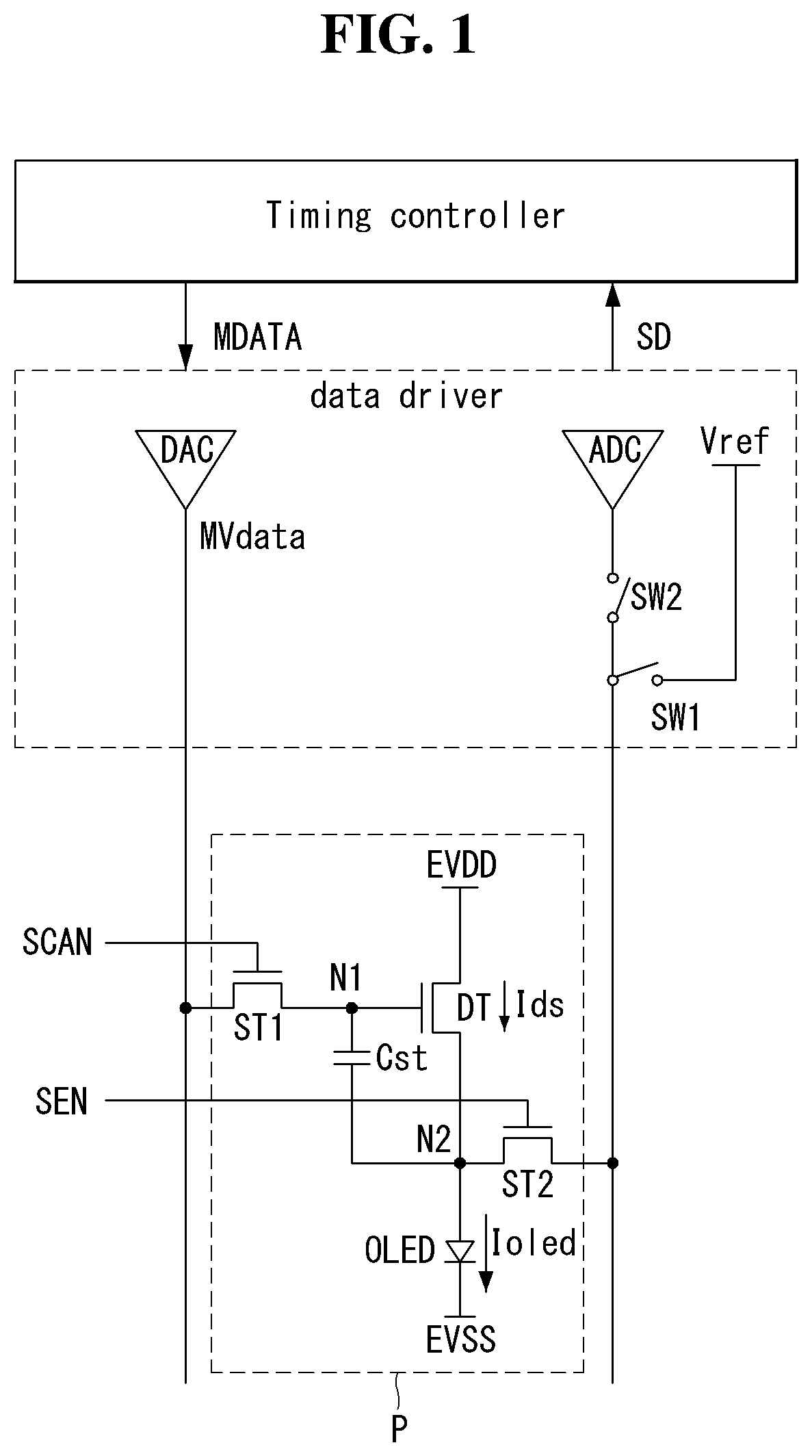
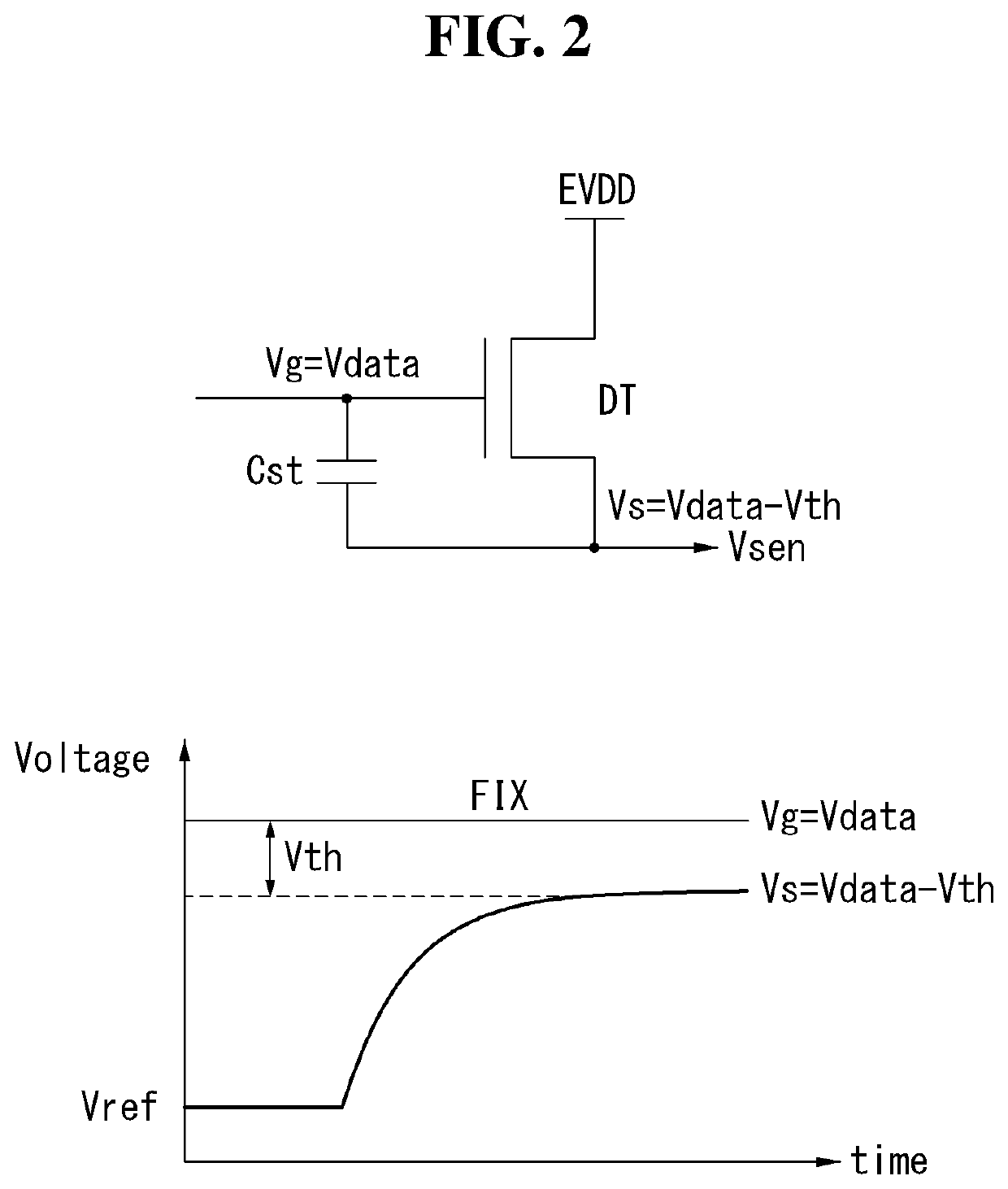
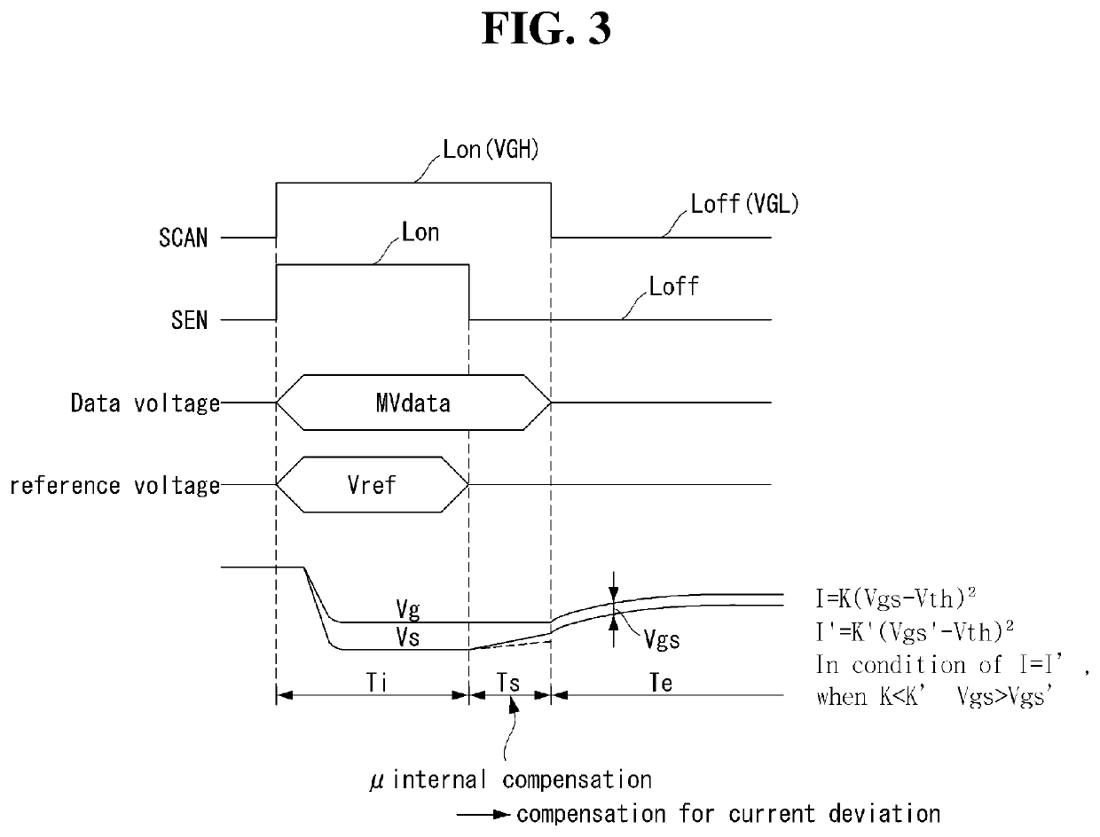
[0042]FIG. 1 shows an equivalent circuit of a sub-pixel to which a hybrid compensation scheme is applied and a data driving circuit, FIG. 2 illustrates a principle in which the threshold voltage change of a driving TFT is compensated, and FIG. 3 is a view for explaining the principle of compensating for the mobility change of the driving TFT.

[0043]Referring to FIG. 1, a subpixel or a pixel P for hybrid compensation may comprise an OLED, a driving TFT DT, a storage capacitor Cst, a first switch TFT ST1, and a second switch TFT ST2. The TFTs constituting th...


PUM

PropertyMeasurementUnit
voltage VGHaaaaaaaaaa
voltage VGLaaaaaaaaaa
voltageaaaaaaaaaa

Abstract

The present disclosure relates to an organic light emitting display device which comprises a plurality of sub-pixels each of which comprises an OLED, a driving TFT, a first TFT for applying a data voltage to a gate electrode of the driving TFT, a second TFT for applying a reference voltage to a source electrode of the driving TFT, and a storage capacitor, a data driver for outputting the data voltage to a data line and the reference voltage to a reference line, and a gate driving unit for outputting signals to a first gate line connected to the gate electrode of the first TFT and a second gate line connected to the gate electrode of the second TFT, wherein two adjacent sub-pixels emitting a same color is supplied with the data voltages through different data lines and share the first gate line and the second gate line.

Description

CROSS-REFERENCE TO RELATED APPLICATION[0001]This application claims the benefit of priority under 35 U.S.C. § 119(a) to Korean Patent Application No. 10-2016-0121665 filed on Sep. 22, 2016, which is incorporated by reference herein in its entirety.BACKGROUND[0002]Field of the Disclosure[0003]The present disclosure relates to a display device, and more particularly, to an organic light emitting display capable of compensating for characteristics of the driving TFTs driving organic-emitting pixels in a structure in which the pixels shares gate lines.[0004]Description of the Background[0005]An active matrix type organic light emitting display is an organic light emitting diode (hereinafter, referred to as “OLED”) which emits light by itself, and has advantages in fast response , high light emitting efficiency, high brightness, and wide viewing angle.[0006]An organic light emitting display device includes pixels each including an OLED and a driving TFT (Thin Film Transistor) in a matrix...

Claims


Application Information

Patent Timeline
Patent Type & Authority Patents(United States)
IPC IPC(8): H01L27/32H01L51/10H01L29/423
CPCH01L29/42312H01L27/3248H01L51/102H01L27/3262H01L27/3211G09G3/3233G09G3/3266G09G2300/0819G09G2310/0205G09G2310/0297G09G2320/0295G09G2320/0233G09G2300/0842G09G2300/0828H10K59/123H10K10/82H10K59/1213H10K59/35
Inventor PARK, HYEMINSHIN, HUNKIKIM, DONGIKLEE, JINWOO
Owner LG DISPLAY CO LTD
Learn More