Non-volatile memory device and method of fabricating the same

a memory device and non-volatile technology, applied in the field of semiconductor devices, can solve the problems of deteriorating the program-erase cycling characteristics of memory cells, affecting the performance of memory cells, and affecting the operation of incremental step pulse programming (ispp) on memory cells, so as to suppress the accumulation of trapped charges, improve data retention performance, and improve the effect of data retention performan

Active Publication Date: 2020-01-28
SK HYNIX INC +1
View PDF18 Cites 0 Cited by
  • Summary
  • Abstract
  • Description
  • Claims
  • Application Information

AI Technical Summary

Benefits of technology

[0006]The present disclosure provides a non-volatile memory device with improved data retention performance and a reliable program-erase cycling characteristic by suppressing accumulation of trapped charges in a space between memory cells in coping with continuous downscaling of the memory cells or multi-level programming of the memory cells.
[0017]According to an embodiment of the present disclosure, a conductive cover layer is formed on sidewalls of a plurality of control gates, the conductive cover layer having a work function that is greater than a work function of the control gates. The conductive cover layer suppresses a magnitude and a dispersion width of a fringing field dispersed from the sidewalls of the control gates to a channel layer, and suppresses tunneling of program charges to inter-memory cell areas of a data storage layer. As a result, accumulation of trapped charges in the inter-memory cell areas is minimized. A non-volatile memory device having improved data retention performance and a reliable program-erase cycling characteristic may be provided.

Problems solved by technology

In this case, when charges stored in a programmed memory cell are lost according to lapse of the time, it is determined that the charges are erased due to reduction of a threshold voltage of the programmed memory cell, and thus a read error may occur.
Furthermore, the program charges moving to or accumulated in inter-memory cell areas of a charge trapping storage layer due to a programming operation, an erasing operation, or a temperature cycling operation, may deteriorate program-erase cycling characteristics of memory cells, and may also deteriorate an incremental step pulse programming (ISPP) operation on memory cells.

Method used


Image

  • Non-volatile memory device and method of fabricating the same
  • Non-volatile memory device and method of fabricating the same
  • Non-volatile memory device and method of fabricating the same

Examples


Embodiment Construction

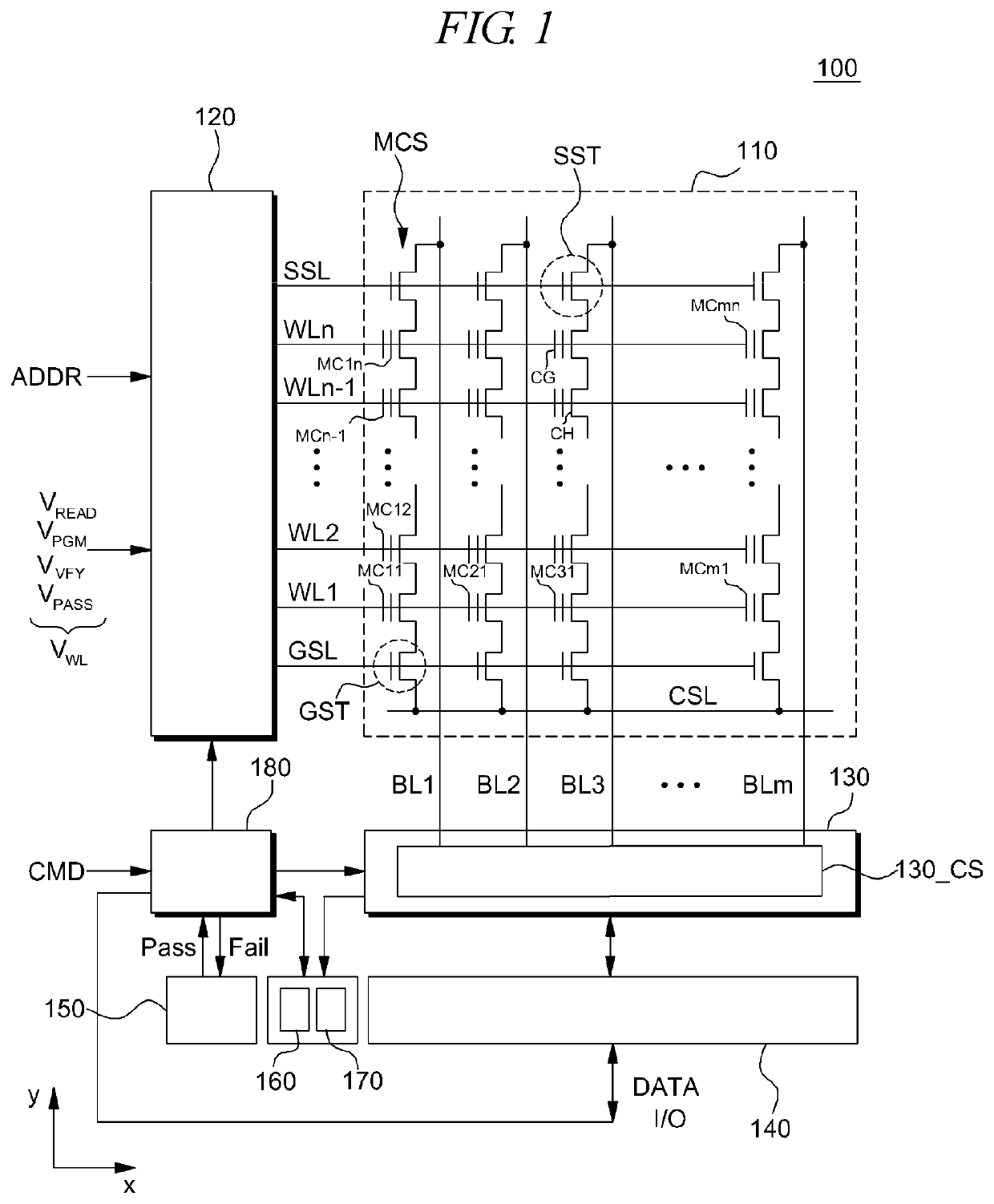
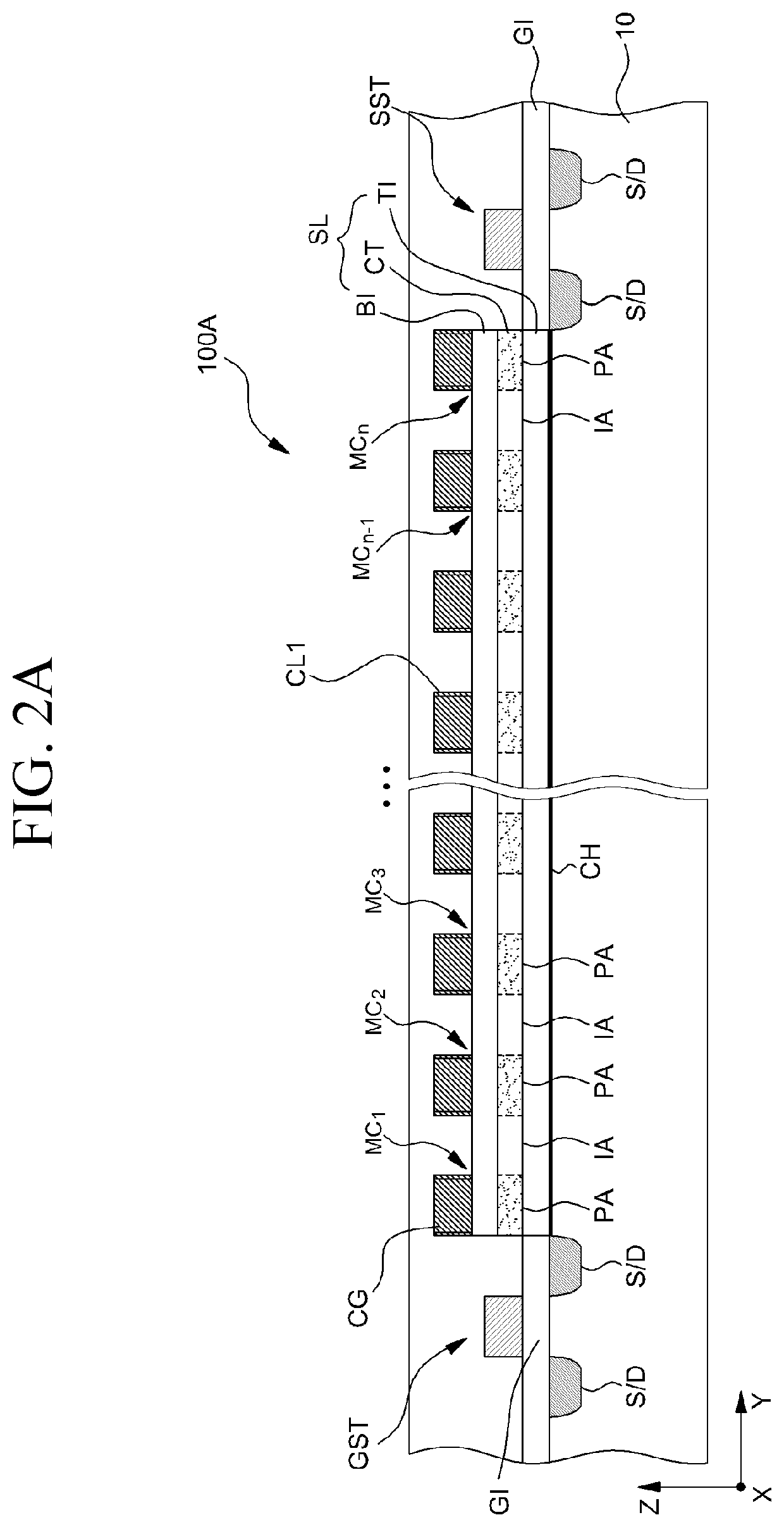
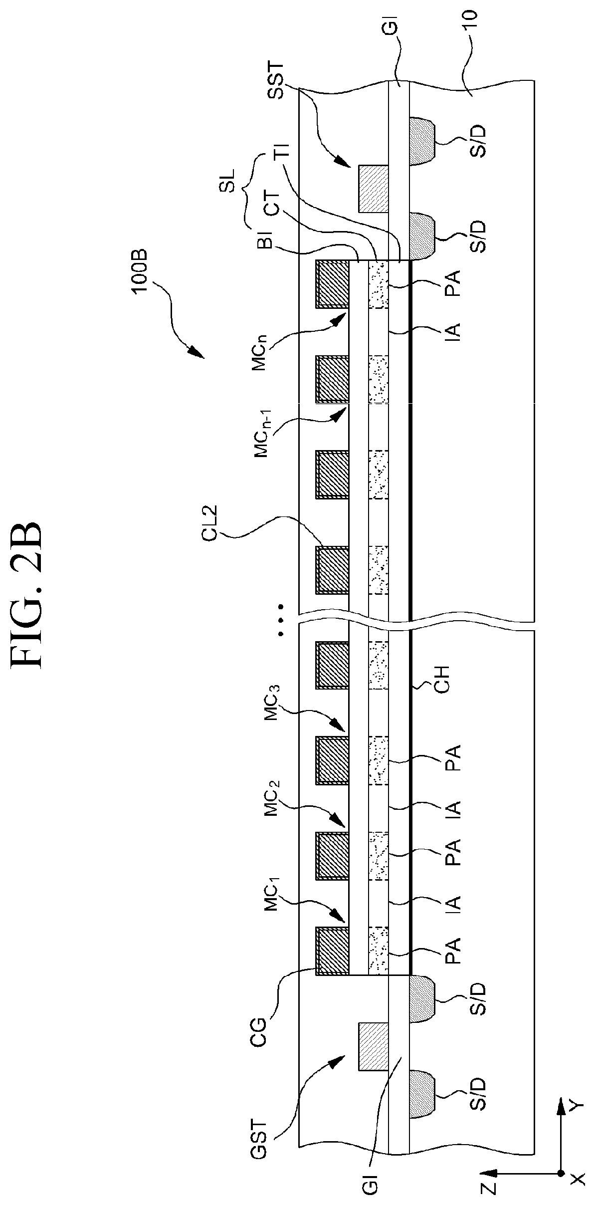
[0037]The present disclosure will now be described more fully with reference to the accompanying drawings, in which exemplary embodiments of the invention are shown. The invention may, however, be embodied in many different forms and should not be construed as being limited to the embodiments set forth herein; rather, these embodiments are provided so that this disclosure will be thorough and complete, and will fully convey the concept of the invention to those skilled in the art.

[0038]Like numbers refer to like elements throughout. As used herein, the term “and / or” includes any and all combinations of one or more of the associated listed items.

[0039]The terminology used herein is for the purpose of describing particular embodiments only and is not intended to be limiting of the invention. As used herein, the singular forms “a”, “an,” and “the” are intended to include the plural forms as well, unless the context clearly indicates otherwise. It will be further understood that the ter...


PUM


Abstract

Provided are a non-volatile memory device and a method of fabricating the same. The non-volatile memory includes a channel layer, a data storage layer disposed on the channel layer, a plurality of control gates arranged on the data storage layer and spaced apart from one another, and conductive cover layers disposed on sidewalls of the control gates facing each other. The plurality of control gates includes a first conductor having a first work function. The conductive cover layers include a second conductor having a second work function that is greater than the first work function.

Description

CROSS-REFERENCES TO RELATED APPLICATION[0001]The present application claims priority under 35 U.S.C. 119(a) to Korean Patent Application number 10-2016-0088850, filed on Jul. 13, 2016, which is herein incorporated by reference in its entirety.BACKGROUND1. Field of the Invention[0002]The present disclosure relates to a semiconductor technique, and more particularly, to a non-volatile memory device and a method of fabricating the same.2. Description of the Related Art[0003]Due to increased demands for portable application devices, such as digital cameras, smart phones, and tablet PCs, markets for non-volatile memory devices are rapidly growing. Non-volatile memory devices include read-only memory (ROM), programmable ROM (PROM), erasable PROM (EPROM), electrically EPROM (EEPROM), and flash memory devices. Among these non-volatile memory devices, flash memory, such as NAND flash memory device, is one of the most prominent non-volatile memory devices contributing to miniaturization and h...

Claims


Application Information

Patent Timeline
Patent Type & Authority Patents(United States)
IPC IPC(8): H01L27/11582H01L27/11568H01L27/115G11C16/04H01L27/1157H01L21/28H01L29/792H01L27/06
CPCH01L27/1157H01L29/40117H01L21/28185H01L27/115G11C16/0475H01L27/11568H01L27/0688H01L29/792H01L27/11582G11C16/0483H10B43/35H10B43/27H01L29/66833H10B43/00H10B43/20H10B43/30H10B69/00
Inventor CHOI, WOO YOUNG
Owner SK HYNIX INC
Why Eureka
Try Eureka