FET driving circuit

a driving circuit and transistor technology, applied in the direction of power conversion systems, oscillation generators, pulse techniques, etc., can solve the problems of increased influence of wiring of mounting patterns, complex design, and fluctuation of switching frequency, so as to reduce the voltage applied, and reduce the voltage of the circuit.

Active Publication Date: 2020-04-21
TDK CORPARATION
View PDF8 Cites 0 Cited by
  • Summary
  • Abstract
  • Description
  • Claims
  • Application Information

AI Technical Summary

Benefits of technology

[0006]The present invention was conceived in view of the problems described above and has a principal object of providing a FET driving circuit that can greatly increase the voltage gradients of rises and falls in a driving waveform supplied to the gate electrode of a FET to be driven (that is, can reduce the time taken by rises and falls in the driving waveform), that has the advantages of a reduced component mounting cost (i.e., a reduced manufacturing cost) and a reduced component mounting area (i.e., miniaturization of the device) by reducing the number of switches while avoiding fluctuations in the switching frequency, and that is capable of operating at high frequency with a lower loss.

Problems solved by technology

However, since the FET driving circuit in Non-Patent Literature 1 described above is self-excited, there is the problem that the design is complex and a further problem in that the switching frequency fluctuates.
Also, since an LC resonance circuit that suppresses the second harmonic component is distributed independently of the components in the driving circuit, there is a problem that the wiring of the mounting pattern has an increased influence when a switching driving operation is performed at high frequency, and due to this influence, there are problems in that it becomes difficult to optimize and stabilize resonant driving operations.
There are also further problems in that it is difficult to reduce the cost of mounting components (i.e., to reduce the manufacturing cost), to minimize the component mounting area (i.e., to miniaturize the device), and to make adjustments to optimize the operation of the device as a whole.
On the other hand, although the FET driving circuit according to Patent Literature 1 mentioned above is externally excited and therefore does not have the problems with the FET driving circuit according to Non-Patent Literature 1 described above (the problems of being complex to design and the switching frequency fluctuating), the FET driving circuit according to Patent Literature 1 requires four switches, which increases the cost of circuitry and since dead time needs to be set to prevent cross conduction, it is difficult to increase the operating frequency.

Method used


Image

  • FET driving circuit
  • FET driving circuit
  • FET driving circuit

Examples


Embodiment Construction

[0037]Several preferred embodiments of the present invention will now be described. Note that the present invention is not limited to the following embodiments. The component elements described below include equivalent component elements that should be apparent to those of skill in the art, and such component elements may be combined as appropriate.

[0038]The embodiments of the present invention will now be described in detail with reference to the drawings. Note that in the description of the drawings, elements that are the same have been assigned the same reference numerals and duplicated description thereof is omitted.

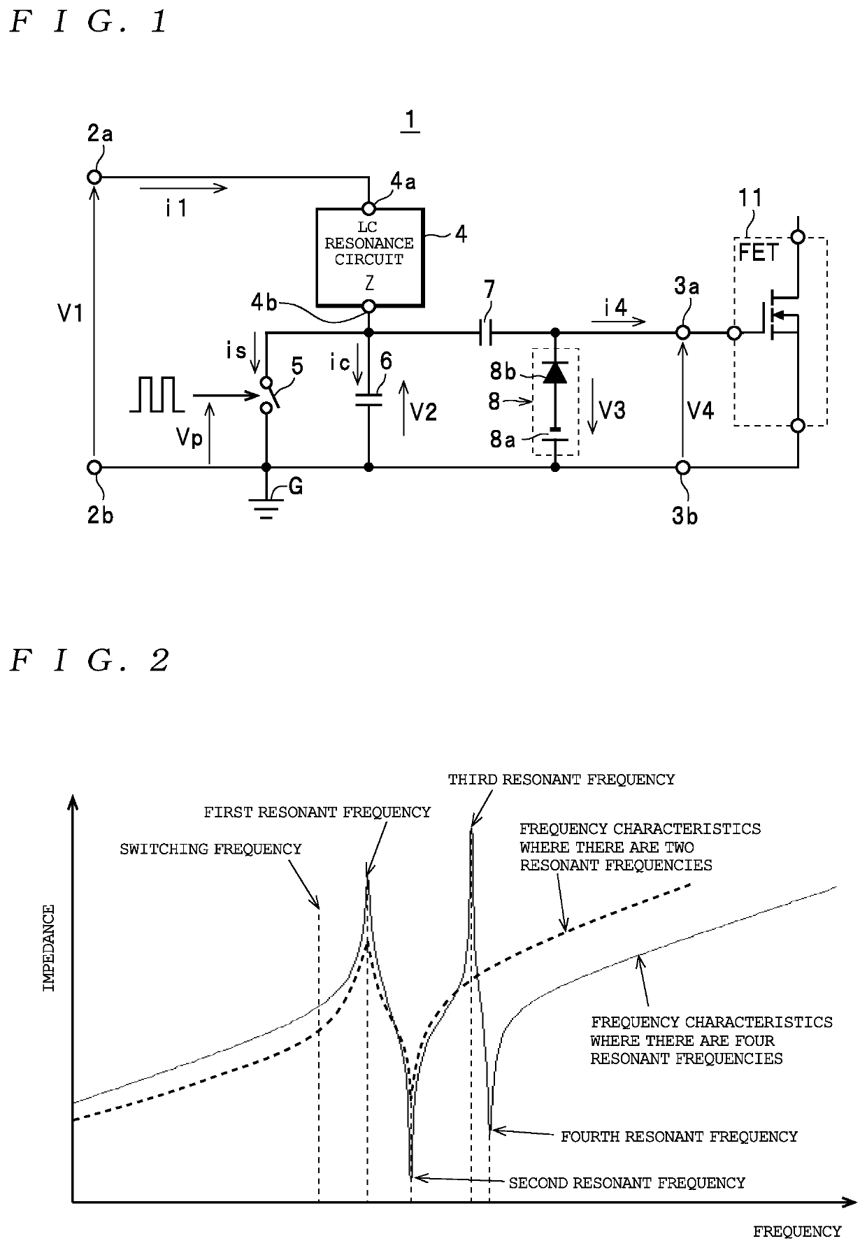
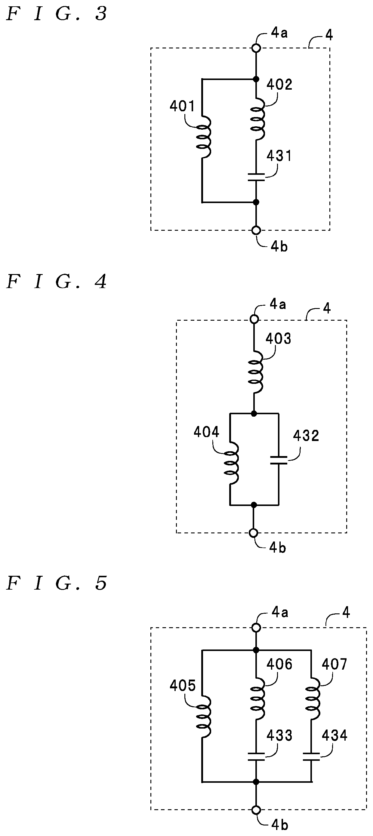
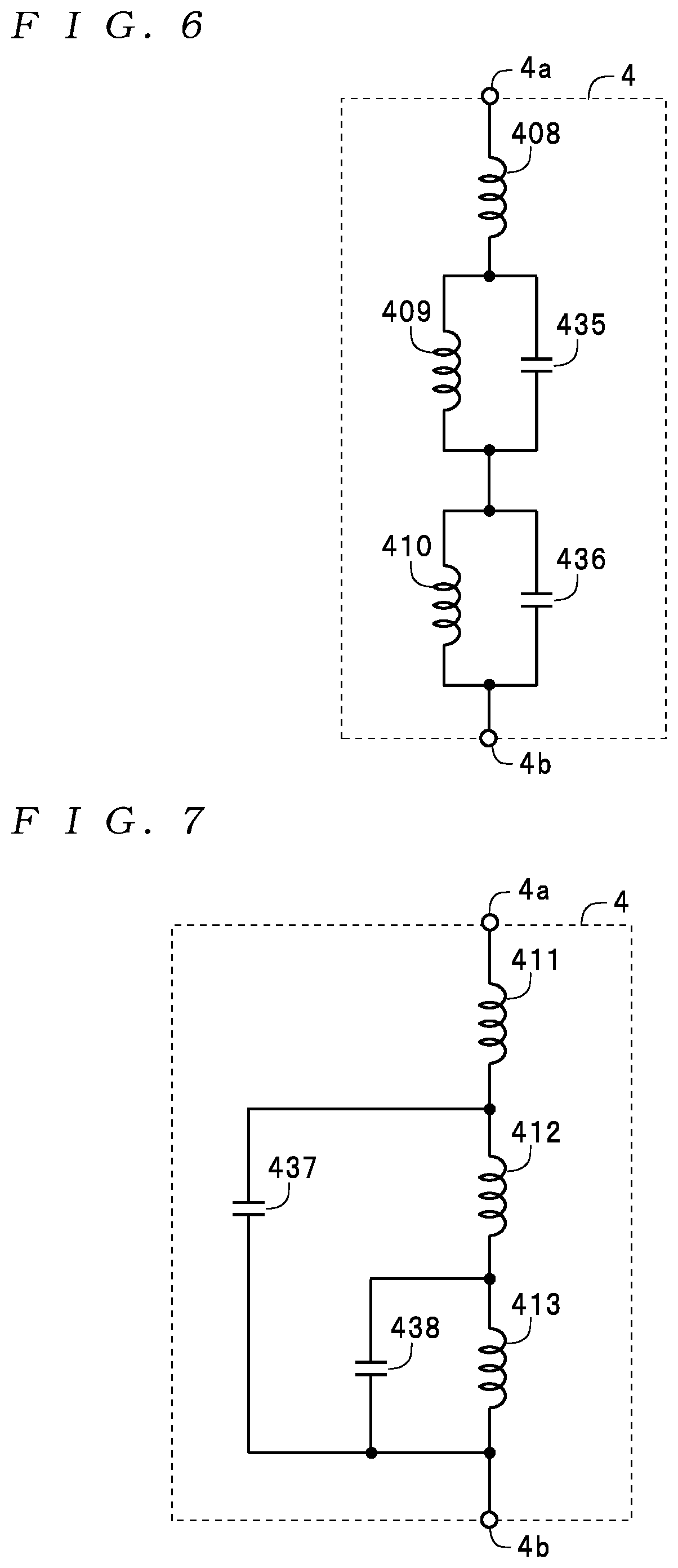
[0039]First, the configuration of a FET driving circuit 1 as one example of a FET driving circuit will be described with reference to FIG. 1.

[0040]The FET driving circuit 1 includes a pair of direct current (DC) input terminals 2a and 2b (hereinafter collectively referred to as the “DC input terminals 2” when no distinction is made), a pair of output terminals 3a and...


PUM


Abstract

A FET driving circuit includes: inputs into which a DC voltage is inputted; outputs connected to gate and source electrodes of a FET; a switch; a capacitance connected across the switch; and an LC resonance circuit connected in series with the switch across the inputs. A voltage generated across the switch during switching is outputted to drive the FET. The LC resonance circuit has a first connector connected to one input and a second connector connected to the switch, and is configured with a path including an inductance and a path including an inductance and a capacitance. An impedance between the first and second connectors has two resonant frequencies. The impedance has a local maximum at the lower resonant frequency, which is higher than a switching frequency, and a local minimum at the higher resonant frequency, which is around double the switching frequency.

Description

FIELD OF THE INVENTION[0001]The present invention relates to a FET (Field Effect Transistor) driving circuit that drives a FET used as a switching element, such as a converter, an inverter, or a switching power supply.DESCRIPTION OF THE RELATED ART[0002]A resonant FET driving circuit is well known as a FET driving circuit for driving a FET (for example, a MOSFET) at a high switching frequency (see Non-Patent Literature 1 (Very-High-Frequency Resonant Boost Converters, IEEE TRANSACTIONS ON POWER ELECTRONICS, VOL.24, NO. 6, JUNE 2009, PP 1654-1665) and Patent Literature 1 (Japanese Translation of PCT International Publication No. 2007-501544)).[0003]Non-Patent Literature 1 discloses a self-excited FET driving circuit which, as depicted in FIG. 5 of the cited document, includes a switch element (MOSFET) connected between the gate electrode and the source electrode of the FET to be driven and an LC resonance circuit that is connected to the gate electrode of the FET to be driven and fun...

Claims


Application Information

Patent Timeline
Patent Type & Authority Patents(United States)
IPC IPC(8): H03K17/687H03K17/0416H03K17/0412H02M1/38H03B5/12
CPCH02M1/38H03K17/04163H03B5/1203H03K17/04123H03K2217/0036H03K2217/009H03F2203/00
Inventor LIN, MINMATSUURA, KEN
Owner TDK CORPARATION
Why Eureka
Try Eureka