
Impedance matching method and device for pulsed radio frequency power supply

a technology of pulsed radio frequency and matching method, which is applied in the direction of plasma technique, electrical equipment, electric discharge tubes, etc., can solve the problems of low matching accuracy, high reflection power (generally 20%) of pulsed rf power supply, and inability to meet the requirements of etching process with a dimension of 22 nm or less, etc., to achieve enhanced processing stability, enhanced utilization of pulsed rf power supply, and enhanced processing stability

Active Publication Date: 2020-05-05
BEIJING NAURA MICROELECTRONICS EQUIP CO LTD
View PDF18 Cites 3 Cited by
  • Summary
  • Abstract
  • Description
  • Claims
  • Application Information

AI Technical Summary

Benefits of technology

[0010]Directed to solving the technical issues existing in the prior art, the present disclosure provides an impedance matching device and a semiconductor processing apparatus that may rapidly realize the impedance matching for the pulsed RF power supply. Accordingly, the processing stability may be enhanced, and the utilization of the RF energy of the pulsed RF power supply may be improved.
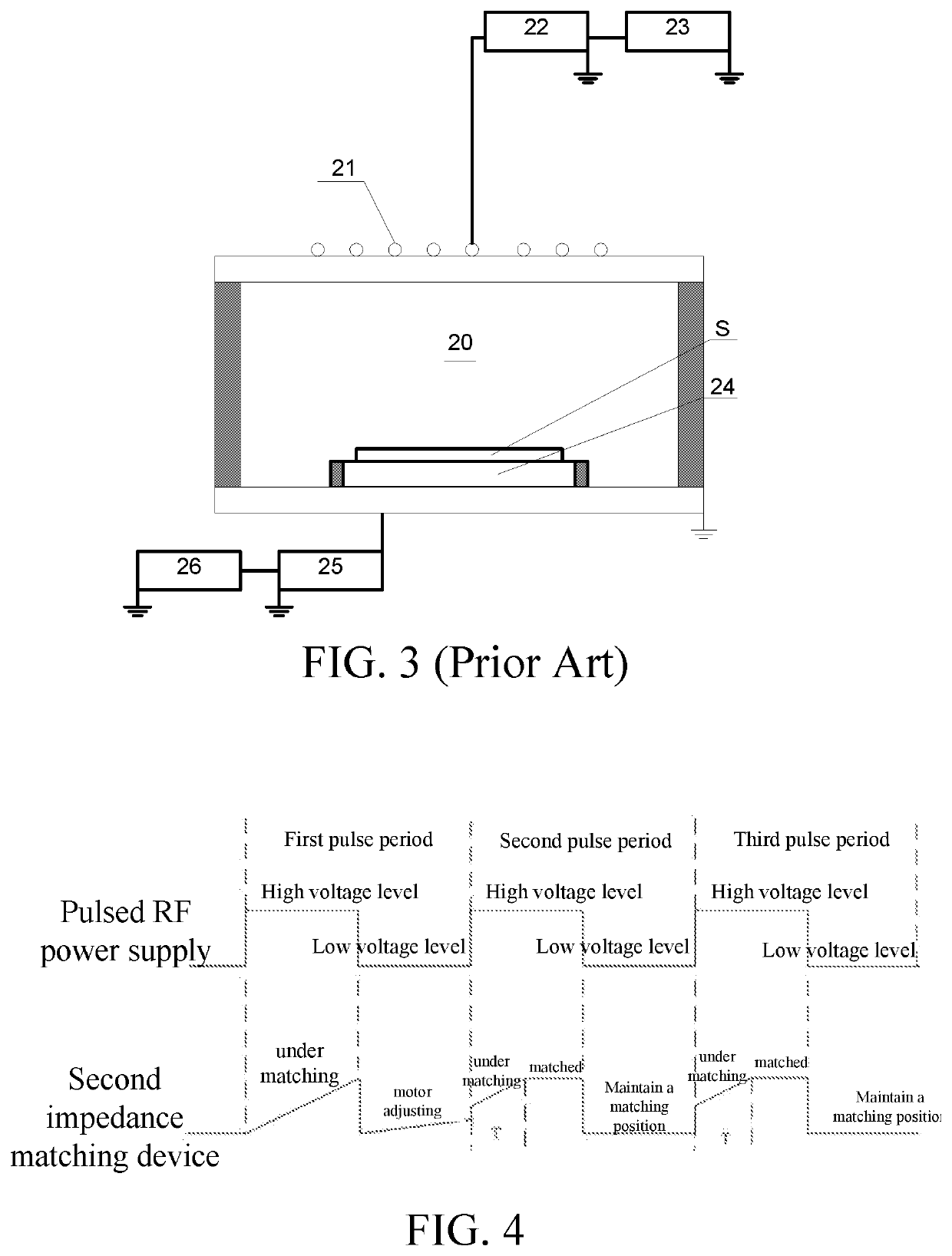
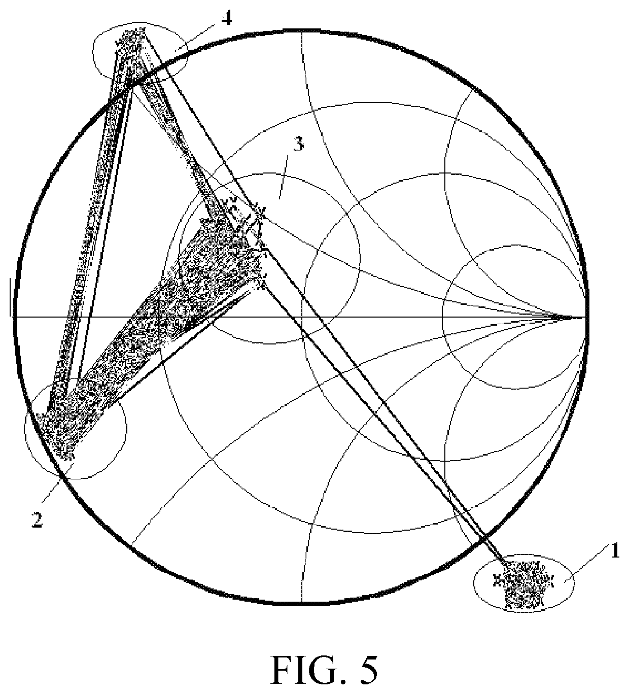
[0027]In the impedance matching method for a pulsed RF power supply provided by the present disclosure, by virtue of the coarse adjustment step, adjustment is performed based on the current load impedance, such that the current reflection coefficient |Γ| is no greater than the ignition reflection coefficient |Γt|, and the current position is set as the ignition position. Further, by virtue of the fine adjustment step, the ignition position remains unchanged, real-time adjustment is performed to realize impedance matching based on the current load impedance, and the current position is set as the matching position. Further by virtue of the switching step, after the impedance matching is realized for the first time, in different pulse time durations in each subsequent pulse period, switching is performed between the ignition position and the matching position. More specifically, in the high voltage level period of each subsequent pulse period, the initial position is switched to the matching position, and in the low voltage level period of each subsequent pulse period, the matching position is switched to the ignition position. Accordingly, ignition may be realized directly in the high voltage level period of the next pulse period, and the re-matching may be realized by switching the ignition position to the matching position. Thus, the matching time of each subsequent pulse period is the switching time between the ignition position and the matching position. As such, different from the matching time of each subsequent pulse period in the prior art being a relatively long time required by the automatic frequency sweeping and repeated adjustments of the load impedance to realize the matching, the processing stability may be enhanced, and utilization of the pulsed RF power supply may be improved.
[0028]In the impedance matching device for a pulsed RF power supply provided by the present disclosure, by virtue of the coarse adjusting unit and based on the current load impedance, the current reflection coefficient |Γ| is adjusted to be no greater than the ignition reflection coefficient |Γt|, and the current position is set as the ignition position. When the current reflection coefficient |Γ| is no greater than the ignition reflection coefficient |Γt|, the fine adjusting unit keeps the ignition position unchanged, performs real-time adjustment to realize impedance matching based on the current load impedance, and sets the current position to be the matching position. Further, the switching unit switches between ignition position and the matching position in different pulse time durations of each subsequent pulse period after the impedance matching is realized for the first time. More specifically, the switching unit switches from the initial position to the matching position in the high voltage level period of each subsequent pulse period, and switches from the matching position to the ignition position in the low voltage level period of each subsequent pulse period, thereby ensuring that the ignition can be realized directly in a high voltage level period of a next pulse period, and re-matching may be realized by switching the ignition position to the matching position. As such, different from the matching time of each subsequent pulse period in the prior art being a relatively long time required by the automatic frequency sweeping and repeated adjustments of the load impedance to realize the matching, the processing stability may be enhanced, and utilization of the pulsed RF power supply may be improved.

Problems solved by technology

As the integrated circuit further develops, the existing technology cannot meet requirements for an etching process with a dimension of 22 nm or less.
Currently, a key factor that restricts the development of the pulsed RF power supply as the plasma excitation source is the impedance matching technique for the pulsed RF power supply.
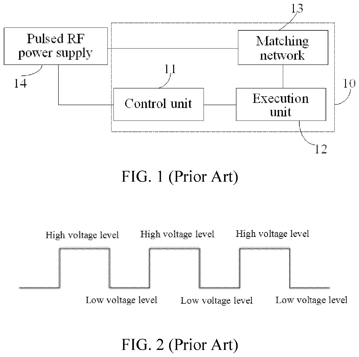
However, by using the existing impedance matching device that relies on the method of mechanical adjustment, impedance matching can hardly be fulfilled within such a few milliseconds, resulting in a low matching accuracy and a high reflection power (generally, 20%) of the pulsed RF power supply.
Thus, the utilization of the pulsed RF power supply is poor.
In practical applications, the following technical issues often exist when the aforementioned existing impedance matching device is used to perform impedance matching on the pulsed RF power supply.
In other words, when using the existing impedance matching device to realize impedance matching, the high voltage level period of each subsequent pulse period needs to undergo a relatively long automatic frequency-sweep matching period T. Thus, the matching efficiency is low, resulting in poor processing stability and low utilization of the pulsed RF power supply.
Therefore, an impedance matching method and device thereof that can implement rapid impedance matching for a pulsed RF power supply are urgently needed.

Method used


Image

  • Impedance matching method and device for pulsed radio frequency power supply
  • Impedance matching method and device for pulsed radio frequency power supply
  • Impedance matching method and device for pulsed radio frequency power supply

Examples


Embodiment Construction

[0041]To make those skilled in the relevant art better understand technical solutions of the present disclosure, an impedance matching method and device thereof for a pulsed RF power supply provided by the present disclosure will be described in detail hereinafter with reference to the accompanying drawings.

[0042]FIG. 6 is a flow chart of an impedance matching method for a pulsed RF power supply provided by a first embodiment of the present disclosure. Referring to FIG. 6, the impedance matching method for a pulsed RF power supply provided by a first embodiment of the present disclosure is used for matching a load impedance of the pulsed RF power supply with a characteristic impedance (e.g., 50 ohms) of the pulsed RF power supply, and the impedance matching method includes the following steps.

[0043]A coarse adjustment step: performing adjustment based on a current load impedance, such that a current reflection coefficient |Γ| is no greater than an ignition reflection coefficient |Γt...


PUM


Abstract

An impedance matching method and device for a pulsed RF power supply are provided. The impedance matching method includes: a coarse adjustment step: performing adjustment based on a current load impedance to make a current reflection coefficient |Γ| no greater than an ignition reflection coefficient |Γt|, and setting a current position as an ignition position; a fine adjusting step: keeping the ignition position unchanged, performing real-time adjustment based on the current load impedance to realize impedance matching, and setting a current position as a matching position; and a switching step: after impedance matching is realized for the first time, switching between the ignition position and the matching position in different pulse time durations of each subsequent pulse period to realize impedance matching in different pulse periods. The impedance matching method and device may improve matching efficiency, process stability and utilization of the pulsed RF power supply.

Description

FIELD OF THE DISCLOSURE[0001]The present disclosure relates to the technical field of semiconductor device manufacturing and, more particularly, relates to an impedance matching method and device for a pulsed radio frequency (RF) power supply.BACKGROUND[0002]A semiconductor processing apparatus often excites a process gas in a reaction chamber to form plasma by applying the RF energy provided by the RF power supply into the reaction chamber with a high vacuum environment. The plasma includes a large amount of active particles, such as electrons, ions, excited atoms, molecules, and free radicals. The active particles react physically and / or chemically with a surface of a wafer exposed to the plasma environment, thereby fulfilling etching, deposition, or other processes of the wafer. As the integrated circuit further develops, the existing technology cannot meet requirements for an etching process with a dimension of 22 nm or less. As such, a pulsed RF power supply is used as a plasma...

Claims


Application Information

Patent Timeline
Patent Type & Authority Patents(United States)
IPC IPC(8): H01J37/32H01L21/02H03H7/40H05H1/46
CPCH01J37/32146H01J37/32H01L21/02H01J37/32183H05H1/46H03H7/40H05H2001/4682H05H2242/26H03H7/38
Inventor CHENG, XIAOYANG
Owner BEIJING NAURA MICROELECTRONICS EQUIP CO LTD
Learn More