High density optical waveguide using hybrid spiral pattern

a hybrid spiral pattern and high-density technology, applied in the direction of optical waveguide light guide, optical light guide, instrument, etc., can solve the problems of large waveguide fabricated in this platform, inability to bend around a tight curve without creating significant optical signal loss, and the resultant size of the device quickly grows

Active Publication Date: 2020-05-26
NAT TECH & ENG SOLUTIONS OF SANDIA LLC
View PDF6 Cites 11 Cited by
  • Summary
  • Abstract
  • Description
  • Claims
  • Application Information

AI Technical Summary

Benefits of technology

[0007]One aspect of the present invention relates to the development of a unique hybrid spiral waveguide geometry that allows for a dense optical waveguide to be implemented without experiencing the signal loss and/or ...

Problems solved by technology

While PLC technology is able to create patterns of waveguides (such as arrays) on a silicon substrate, the waveguides fabricated in this platform are relatively large and unable to bend around a tight curve without creating significant optical signal loss (i.e., a tight bend tends to disru...

Method used


Image

  • High density optical waveguide using hybrid spiral pattern
  • High density optical waveguide using hybrid spiral pattern
  • High density optical waveguide using hybrid spiral pattern

Examples


Embodiment Construction

[0027]As mentioned above, it is frequently desirable to be able to reduce the physical size of an AWG, either to be able to fit more functions on a chip or to fabricate smaller chips. There are physical limits on how small a conventional AWG can be made, however, since waveguide curves must be made gentle enough to maintain their guiding properties. A significant amount of space is also consumed by the input and output waveguides, which must fan-in or fan-out to direct the light to or from the edges of the chip.

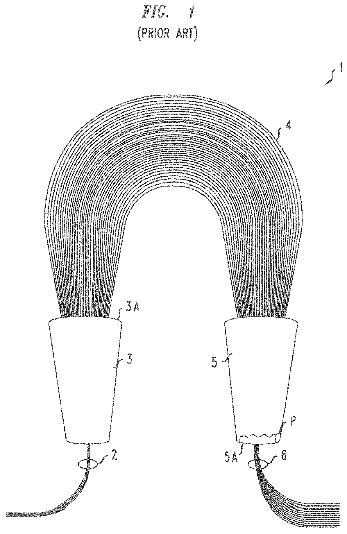
[0028]FIG. 1 illustrates the layout of a conventional AWG. It comprises a substrate (“die”, “chip”) 1 supporting one or more input optical waveguides 2 delivering optical energy into an “input slab” region 3. The slab region is a planar waveguide which confines the input optical energy in only the vertical dimension; the energy is permitted to spread transversely without restriction. The input slab is sometimes referred to as an “input free space region”, or an “input free pr...


PUM


Abstract

A hybrid spiral waveguide geometry is proposed that exhibits essentially zero curvature (i.e., infinite bend radius) at the center of the spiral (similar to a Fermat spiral), with the curvature then increasing in value as the spiral moves outward. Advantageously, as the spiral moves away from the center, the spacing between adjacent waveguides quickly approaches a constant value (similar to an Archimedean spiral). This hybrid spiral structure has been found to allow for a high density waveguide to be created with lower loss and requiring a smaller size than many conventional spiral configurations and finds use in optical delay lines, amplifiers and arrayed waveguide gratings.

Description

REFERENCE TO RELATED APPLICATION[0001]This application is a continuation-in-part of prior application Ser. No. 15 / 782,710, which was filed on Oct. 12, 2017 by Michael Gehl et al. under the title, “High Density Optical Waveguide Using Hybrid Spiral Pattern”, and which is commonly owned herewith. The entirety of the above said application Ser. No. 15 / 782,710 is hereby incorporated herein by reference.STATEMENT OF GOVERNMENT SUPPORT[0002]This invention was made with Government support under Contract DE-NA0003525 awarded by the United States Department of Energy / National Nuclear Security Administration. The U.S. Government has certain rights in the invention.BACKGROUND[0003]There are a variety of optical communication system applications that utilize optical waveguides of varying lengths, or simply require the use of relatively long waveguides. For example, optical delay lines are typically based on configurations having two separate optical waveguide paths, with one path having an “opt...

Claims


Application Information

Patent Timeline
IPC IPC(8): G02B6/125G02F1/01G02B6/12
CPCG02B6/125G02F1/011G02B6/12G02B6/12033G02B6/12009G02F1/0147G02B2006/12097G02B2006/12142G02B2006/12061G02B2006/12085G02B6/122
Inventor GEHL, MICHAELDEROSE, CHRISTOPHER
Owner NAT TECH & ENG SOLUTIONS OF SANDIA LLC
Why Eureka
Try Eureka