Thin film transistor array substrate, method of manufacturing the same, and display device including thin film transistor substrate

a technology of thin film transistors and array substrates, which is applied in the field of thin film transistor array substrates, can solve the problems of high cost of the device used by this method, low defect state density of poly-si, and difficulty in manufacturing a large area of poly-si thin films, so as to reduce the crystallization temperature of a-si thin films, avoid deformation of the base substrate due to high temperature, and shorten the crystallization time

Active Publication Date: 2020-06-23
SHENZHEN CHINA STAR OPTOELECTRONICS SEMICON DISPLAY TECH CO LTD
View PDF10 Cites 0 Cited by
  • Summary
  • Abstract
  • Description
  • Claims
  • Application Information

AI Technical Summary

Benefits of technology

[0006]For this purpose, the present disclosure provides a method of manufacturing a thin film transistor (TFT) array substrate, which adopts solid-phase crystallization (SPC) to manufacture a poly-Si thin film as an active layer. The method may reduce a crystallization temperature and avoid deformation of a base substrate while shortening crystallization time and improving production efficiency.
[0030]The method of manufacturing the TFT array substrate provided in the embodiment of the present disclosure adopts the SPC to manufacture the poly-Si thin film as the active layer, wherein the B-doped a-SiGe thin film layer is manufactured on the a-Si thin film layer. The B-doped a-SiGe thin film layer may induce the a-Si thin film layer to be converted into the poly-Si thin film while performing the SPC, thereby reducing the crystallization temperature of the a-Si thin film and shortening the crystallization time thereof. Thus, the deformation of the base substrate due to the high temperature is avoided, and the production efficiency is improved.

Problems solved by technology

If the poly-Si is manufactured using the ELA, the poly-Si has low defect state density, and it is difficult to manufacture a large area of the poly-Si thin film; in addition, the device used by this method is expensive, and the cost is high.
In the poly-Si thin films manufactured using the MIC and MILC, there is much metal residual, so that characteristics of the TFT become worse.
However, if this method is applied to manufacturing the TFT array substrate, since a base substrate is easily deformed at high temperature, it needs to set a temperature of the crystallization lower, and the reduction of the crystallization temperature causes crystallization time to be greatly increased, thereby reducing production efficiency.

Method used


Image

  • Thin film transistor array substrate, method of manufacturing the same, and display device including thin film transistor substrate
  • Thin film transistor array substrate, method of manufacturing the same, and display device including thin film transistor substrate
  • Thin film transistor array substrate, method of manufacturing the same, and display device including thin film transistor substrate

Examples


Embodiment Construction

[0034]In order for the purpose, technical solution and advantages of the present disclosure to be clearer, the embodiments of the present disclosure will be explained in details below in conjunction with the drawings. The preferred embodiments are exemplified in the drawings. The embodiments of the present disclosure as shown in the drawings and as described according to the drawings are only exemplified, and the present disclosure is not limited to these embodiments.

[0035]Here, it is also worthy to note that, in order to prevent the present disclosure from being obscured due to unnecessary details, the drawings only illustrate the structure and / or processing steps closely related to the solution based on the present disclosure, while other details less related to the present disclosure are omitted.

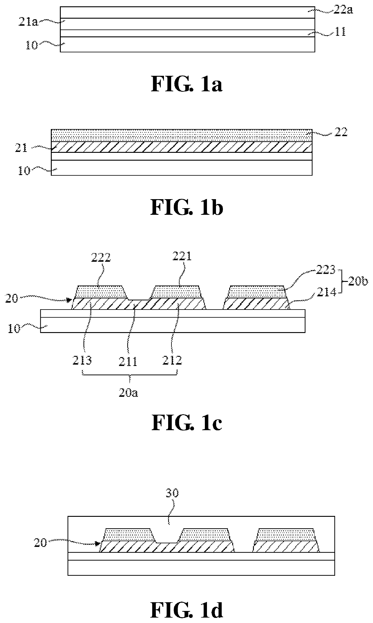
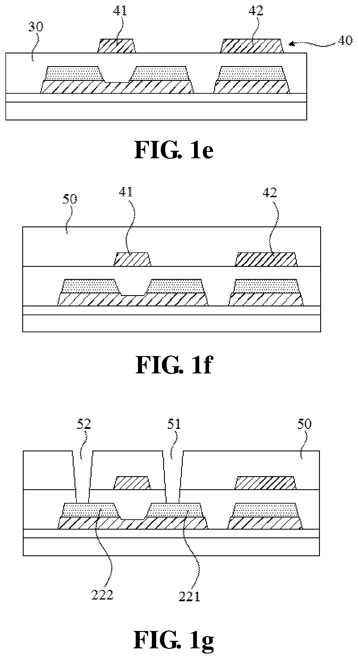
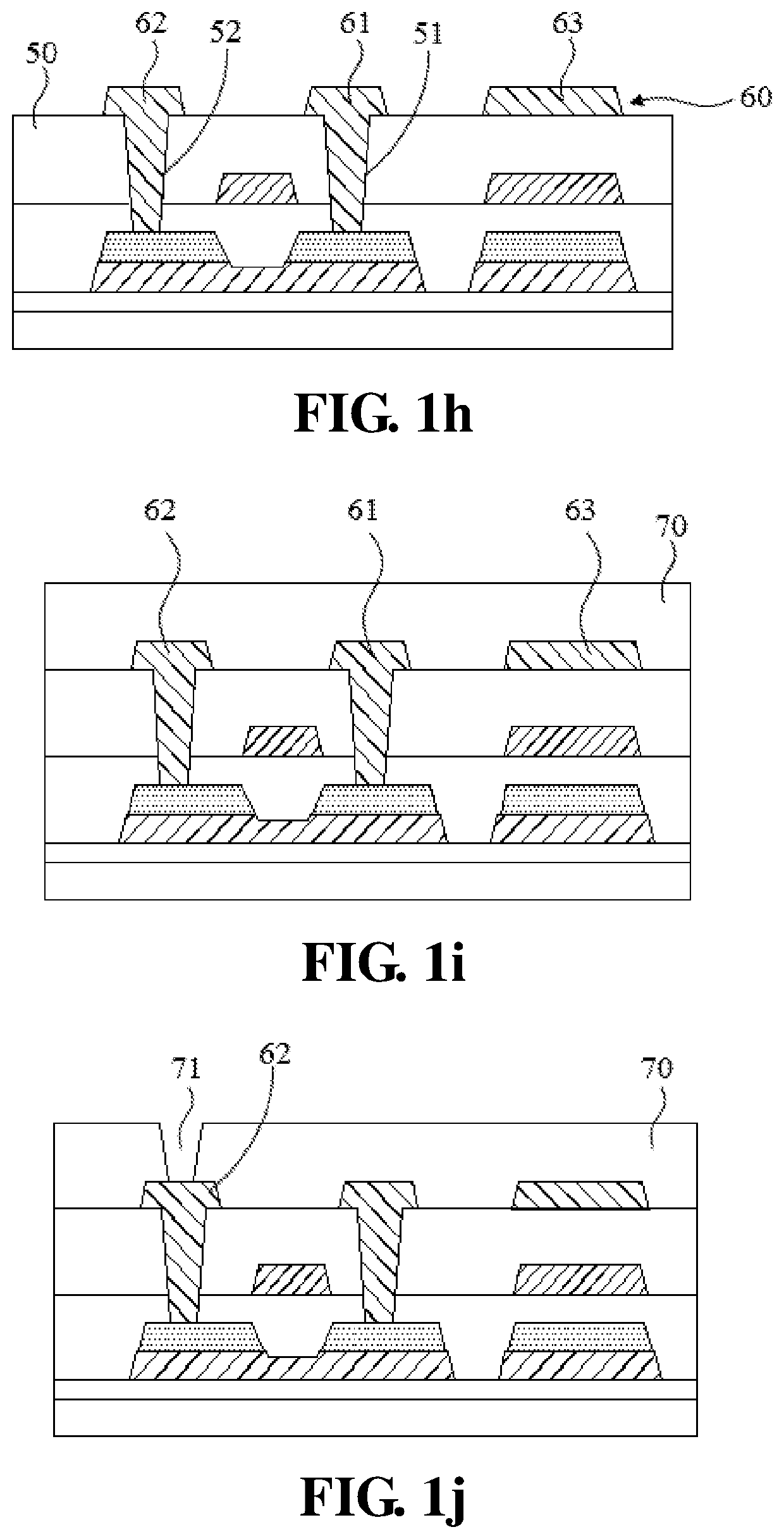
[0036]The present disclosure firstly provides a method of manufacturing a thin film transistor (TFT) array substrate. Referring toFIGS. 1a-1k, the method includes the following steps.

[003...


PUM

PropertyMeasurementUnit
temperatureaaaaaaaaaa
thicknessaaaaaaaaaa
Thicknessesaaaaaaaaaa

Abstract

The present disclosure discloses a method of manufacturing a thin film transistor (TFT) array substrate including a step of preparing a patterned active layer on a base substrate, wherein the step includes: sequentially forming an amorphous silicon (a-Si) thin film layer and a boron-doped (B-doped) amorphous silicon germanium (a-SiGe) thin film layer on the base substrate; performing crystallization on the a-Si thin film layer and the B-doped a-SiGe thin film layer using a thermal annealing process to obtain a polycrystalline silicon (poly-Si) thin film layer and a B-doped polycrystalline silicon germanium (poly-SiGe) thin film layer; and forming the patterned active layer by using a photolithography process to etch the poly-Si thin film layer and the B-doped poly-SiGe thin film layer. The present disclosure further discloses a TFT array substrate and a display device including the TFT array substrate.

Description

CROSS-REFERENCES TO RELATED APPLICATION[0001]This application is a U.S. national phase application, pursuant to 35 U.S.C. § 371, of PCT / CN2017 / 093424, filed Jul. 18, 2017, designating the United States, which claims priority to Chinese Application No. 201710508076.9, filed Jun. 28, 2017. The entire contents of the aforementioned patent applications are incorporated herein by this reference.TECHNICAL FIELD[0002]The present disclosure relates to the technical field of a display, and in particular, to a thin film transistor array substrate, a method of manufacturing the same, and a display device including the thin film transistor array substrate.BACKGROUND ART[0003]Flat-panel display devices have numerous advantages of thin body, power saving, no radiation and so on, and thus are widely applied. The current flat-panel display devices mainly include liquid crystal display (LCD) devices, and organic light emitting display (OLED) devices. A thin film transistor (TFT) is a significant com...

Claims


Application Information

Patent Timeline
Patent Type & Authority Patents(United States)
IPC IPC(8): H01L29/786H01L27/12H01L21/02
CPCH01L29/78618H01L27/1274H01L27/1255H01L29/78675H01L21/02667H01L21/0262H01L21/02532H01L21/02592H01L27/1222H01L27/1259H01L27/1277H01L27/1281H01L21/02579H01L21/02488H01L21/0245H01L21/02502H01L29/66757H01L29/78684
Inventor ZHOU, XINGYU
Owner SHENZHEN CHINA STAR OPTOELECTRONICS SEMICON DISPLAY TECH CO LTD
Why Eureka
Try Eureka