

Power amplifier circuit
a power amplifier and circuit technology, applied in the direction of rf amplifiers, amplifiers with semiconductor devices/discharge tubes, high frequency amplifiers, etc., can solve the problem that the power amplifier circuit may not achieve desirable efficiency over a wide output power rang
- Summary
- Abstract
- Description
- Claims
- Application Information
AI Technical Summary
Benefits of technology
Problems solved by technology
Method used
Image

Examples
first embodiment
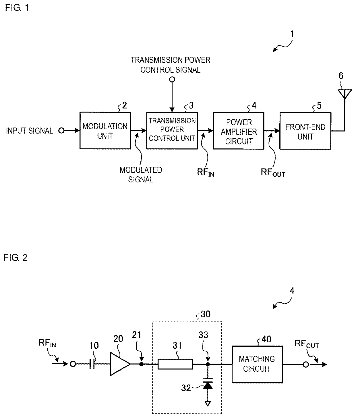
[0029]FIG. 1 illustrates a configuration of a transmission unit including a power amplifier circuit according to a first embodiment. A transmission unit 1 is used in, for example, a mobile communication device, such as a cellular phone, to transmit various signals, such as voice and data, to a base station. Although the mobile communication device also includes a reception unit for receiving signals from the base station, description of the reception unit is omitted herein.
[0030]As illustrated in FIG. 1, the transmission unit 1 includes a modulation unit 2, a transmission power control unit 3, a power amplifier circuit 4, a front-end unit 5, and an antenna 6.
[0031]The modulation unit 2 outputs, to the transmission power control unit 3, a radio frequency (RF) modulated signal obtained by modulating an input signal on the basis of a modulation system, such as a high speed uplink packet access (HSUPA) system or a long term evolution (LTE) system. As an example, the frequency of the mod...
second embodiment
[0064]FIG. 6 illustrates a configuration of a power amplifier circuit according to a second embodiment. Components that are the same as those in the first embodiment are denoted by the same reference numerals, and description thereof is omitted.
[0065]A power amplifier circuit 4A includes the capacitor 10, the amplifier 20, the matching circuits 30 and 40, and a bias circuit 50.
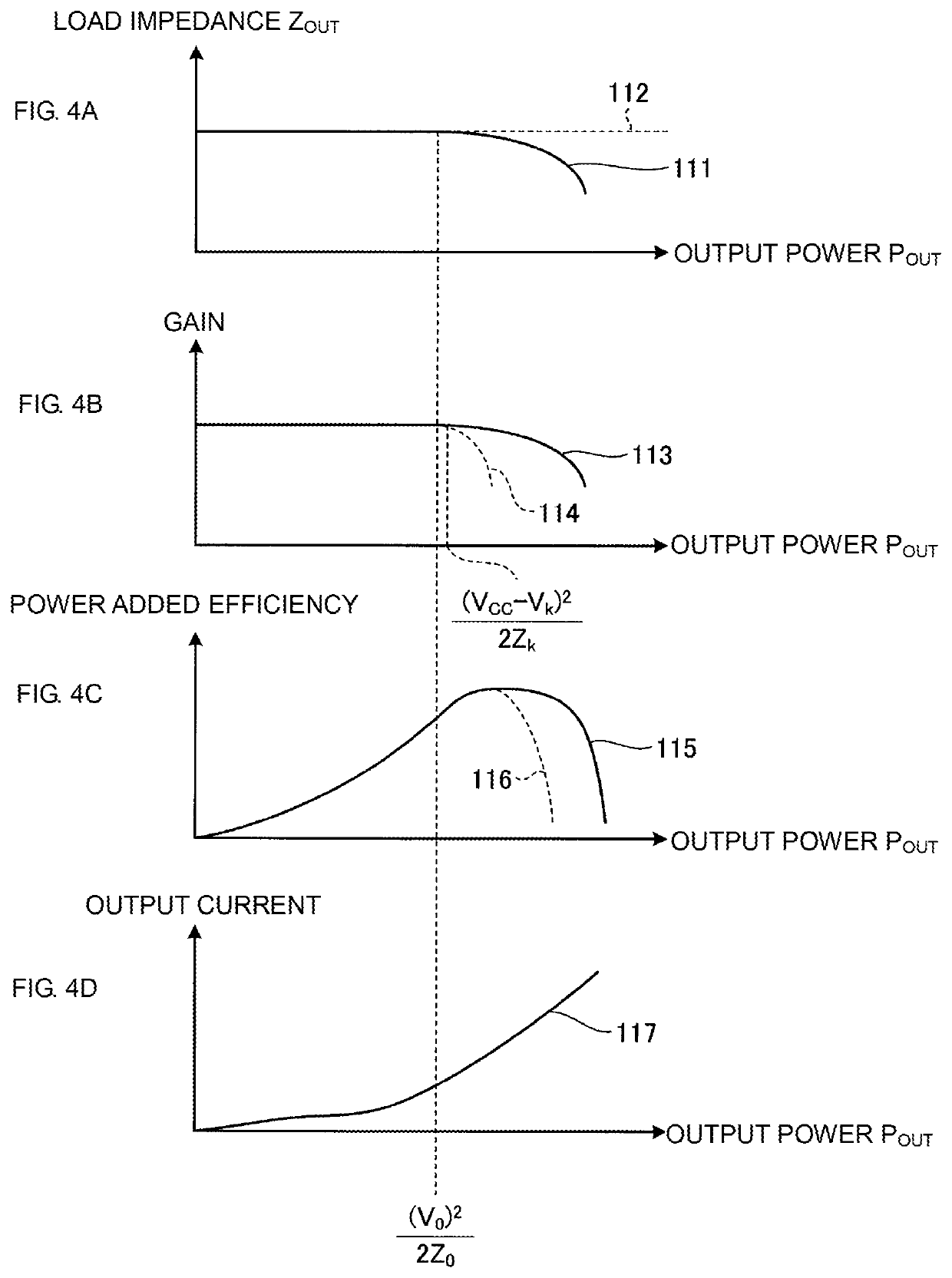
[0066]As an example, the amplifier 20 includes a transistor Q1 and a direct-current choke inductor L3. Although an example of the transistor Q1 is an NPN-type heterojunction bipolar transistor (HBT), the transistor Q1 is not limited to this. An emitter of the transistor Q1 is connected to the reference potential. The radio frequency input signal RFIN having passed through the capacitor 10 is supplied to a base of the transistor Q1. A collector of the transistor Q1 is connected to the first node 21. In the case where the transistor Q1 is the NPN-type HBT, a minimum voltage Vk at which the amplifier 20 operates ...
third embodiment
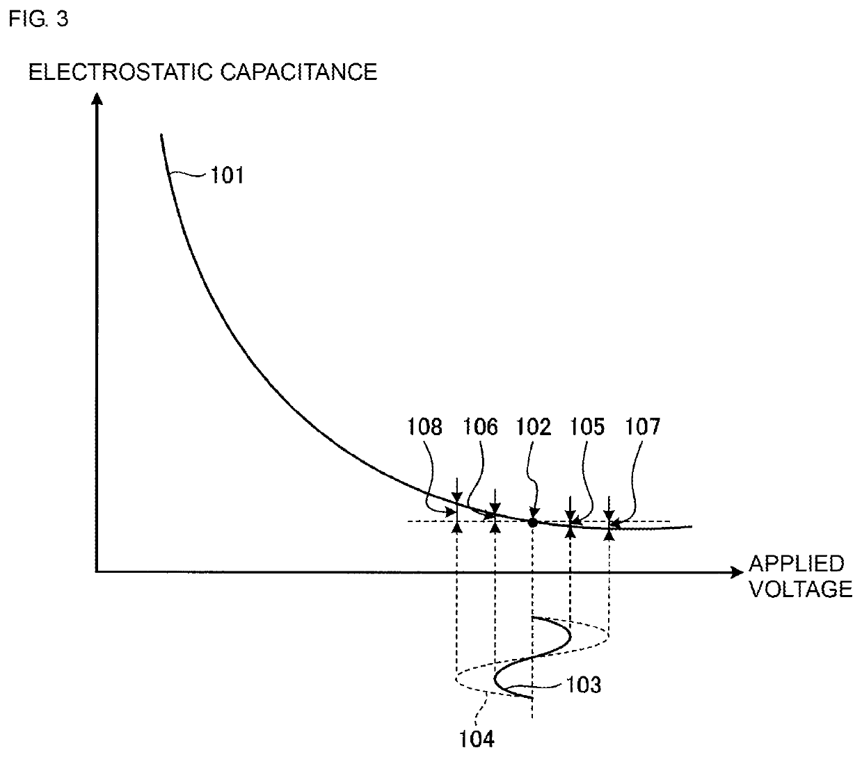
[0106]FIG. 14 illustrates a configuration of a variable capacitor of a power amplifier circuit according to a third embodiment. The entire configuration of the power amplifier circuit according to the third embodiment is the same as that of the power amplifier circuit 4A according to the second embodiment, and an illustration and description thereof are omitted. Furthermore, components that are the same as those in the first or second embodiment are denoted by the same reference numerals, and description thereof is omitted.
[0107]The variable capacitance element VC1 of a variable capacitor 32A includes a transistor Q11. Although an example of the transistor Q11 is an NPN-type HBT, the transistor Q11 is not limited to this. For example, the transistor Q11 may be a PNP-type HBT. A base and an emitter of the transistor Q11 are connected to the reference potential. A collector of the transistor Q11 is connected to the second node 33. That is, the variable capacitance element VC1 is a bas...
PUM
 Abstract
Description
Claims
Application Information