On-wafer calibration device

a technology of calibration device and wafer, which is applied in the manufacture of electrical instruments, electronic circuit testing, instruments, etc., can solve the problems of inadequacies in the most efficient and accurate way of on-wafer calibration of vector network analyzer, and the calibration technique is not suitable to accurately measure integrated devices on wafer, and achieves low loss and high isolation

Active Publication Date: 2020-10-06
ROHDE & SCHWARZ GMBH & CO KG
View PDF8 Cites 0 Cited by
  • Summary
  • Abstract
  • Description
  • Claims
  • Application Information

AI Technical Summary

Benefits of technology

[0018]According to a further preferred implementation form of the first aspect, the diode is an aluminum gallium arsenide diode, especially an aluminum gallium arsenide PIN diode. Advantageously, such diodes provide low loss and high isolation.
[0019]According to a further preferred implementation form of the first aspect, the on-wafer calibration device comprises a coating based on benzocyclobutene above the substrate. Advantageously, the on-wafer calibration device is protected against environmental and mechanical influences to ensure long term durability and handling ruggedness.

Problems solved by technology

As this calibration matrix comprises cabling and has quite large structures with respect to radio frequency signals, it is therefore not suitable for an on-wafer calibration of a vector network analyzer in a most efficient and accurate manner.
Thus, the calibration technique is not appropriate to accurately measure integrated devices on wafer.

Method used


Image

  • On-wafer calibration device
  • On-wafer calibration device
  • On-wafer calibration device

Examples


Embodiment Construction

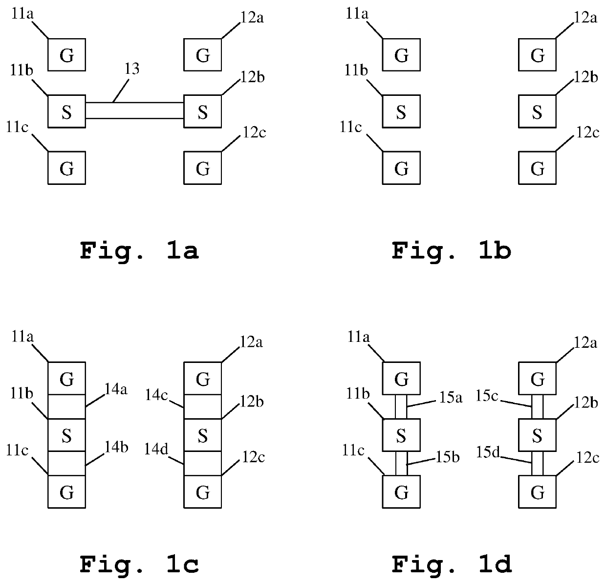
[0036]Firstly, each of the FIGS. 1a to 1d illustrates an exemplary embodiment of a calibration standard. Each of these calibration standards exemplarily comprises two measuring ports.

[0037]In each case according to the FIGS. 1a to 1d, a first measuring port comprises a first ground pad 11a, especially a probe tip pad connected to ground, a signal pad 11b, especially a probe tip pad being connectable to a first measuring signal, and a second ground pad 11c, especially a probe tip connected to ground.

[0038]By analogy with the first measuring port described above, in each case according to the FIGS. 1a to 1d, a second measuring port comprises another first ground pad 12a, especially a probe tip pad connected to ground, another signal pad 12b, especially a probe tip pad being connectable to a second measuring signal, and another second ground pad 12c, especially a probe tip pad connected to ground.

[0039]In this context, it is noted that each measuring port may alternatively comprise an ...


PUM

PropertyMeasurementUnit
impedanceaaaaaaaaaa
impedanceaaaaaaaaaa
cut-off frequencyaaaaaaaaaa

Abstract

An on-wafer calibration device comprises on a substrate at least a first measuring port, at least a first switch element, at least two calibration standards, and a controller unit or a control interface for control of the first switch element. The first switch element is controlled in a manner that it selectively connects a wafer probe tip connectable to the first measuring port to the at least two calibration standards.

Description

TECHNICAL FIELD[0001]The invention relates to an on-wafer calibration device, especially an on-wafer calibration device on a substrate, for calibrating measuring devices, especially vector network analyzers.BACKGROUND ART[0002]Generally, in times of an increasing number of applications employing electrical circuits, especially integrated radio frequency circuitry, there is a growing need of well-calibrated measuring devices such as vector network analyzers for testing said circuitry on wafer, and thus a particular need of a calibration device for calibrating said measuring devices in a most efficient and accurate manner with a reference plane located on wafer.[0003]DE 10 2005 018 073 A1 discloses a multi-gate calibration matrix for calibration of multi-gate network analyzers. As this calibration matrix comprises cabling and has quite large structures with respect to radio frequency signals, it is therefore not suitable for an on-wafer calibration of a vector network analyzer in a mo...

Claims


Application Information

Patent Timeline
Patent Type & Authority Patents(United States)
IPC IPC(8): G01N21/93G01R35/00H01L21/67G01R3/00H01L21/673H01L21/66G01R31/28G01R27/28
CPCH01L22/34G01R3/00G01R35/005G01R31/2856H01L21/67011H01L21/67356G01N21/93G01R27/28
Inventor ZIEGLER, ROBERT
Owner ROHDE & SCHWARZ GMBH & CO KG
Why Eureka
Try Eureka