
Assembly platform

a technology of assembly platform and nanostructure, which is applied in the direction of electrical apparatus, semiconductor devices, semiconductor/solid-state device details, etc., can solve the problems of limiting limiting the form factor and/or the performance of a final electronic device, and the potential of the today's conventional interposer facing the limitations of the number of devices that can be connected, etc., to achieve the effect of reducing the size of the complete electronic assembly, reducing the distance of the bump

Active Publication Date: 2020-11-17
SMOLTEK AB
View PDF27 Cites 0 Cited by
  • Summary
  • Abstract
  • Description
  • Claims
  • Application Information

AI Technical Summary

Benefits of technology

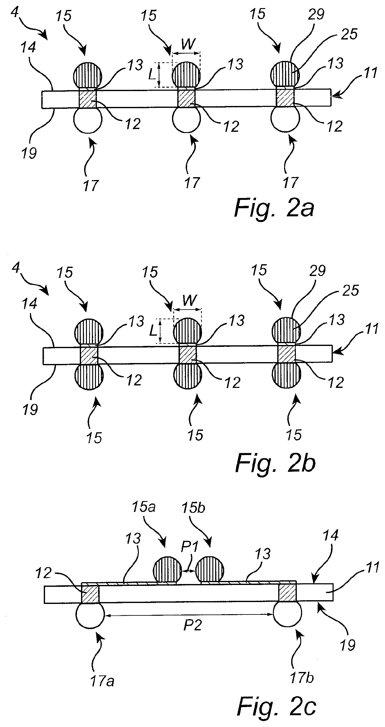
[0011]The term “nanostructure connection bump” is not meant to mean that the connection bump itself has to be nano-sized, but is meant to mean that the connection bump comprises nanostructures. The present invention is based upon the realization that an assembly platform can conveniently be provided using nanostructures embedded in a metal as nanostructure connection bumps. By growing the nanostructures on the assembly substrate, the pitch, i.e. the distance between the nanostructure connection bumps can be considerably reduced compared to conventional connection bumps, thereby enabling more input / output points on an assembly platform (i.e. the density of I / O's can be increased). Additionally, the height of the assembly platform as an interposer in the direction of the interconnected devices (i.e. IC and substrate) can be reduced compared to conventional interposers, thereby reducing the size of the complete electronic assembly. Furthermore, the assembly platform can be processed at higher temperatures than typical integrated circuits, allowing larger thermal budget window and thereby more freedom in the configuration of the nanostructures and / or a more cost-efficient processing. In addition, manufacturing of the assembly platform is significantly simplified by growing the nanostructures on the assembly substrate since the nanostructures do not have to be e.g. transferred or otherwise additionally processed. A further advantage is that the interface strength / properties between the nanostructures and the underlying substrate is improved by growing the nanostructures directly on the substrate or on the electrode. Another additional advantage to grow the nanostructures directly on the assembly substrate or on the electrode present on the substrate is that the growth processing parameters for growing nanostructures do not need to comply with the traditional CMOS or other chip processing environments open up new possibilities. Furthermore, growth processing parameters can be tailored to grow nanostructures with different properties. This can enable to exploit the electrical, mechanical, optical or any other properties of grown nanostructures to benefit the assembly platform.
[0012]The use of grown nanostructures allows extensive tailoring of the properties of the nanostructures. For instance, the height of the assembly platform may be controlled by tailoring the growing height of the nanostructures. Such advantage essentially may unleash the control of the size of a nanostructure bumps to be controlled in all x, y and z directions.
[0017]According to embodiments, the plurality of elongated nanostructures of the nanostructure connection bump and the amount of metal may be configured so that the metal is maintained within the connection location by the plurality of elongated nanostructures. The nanostructures may thus be arranged to cause capillary forces that prevent the metal from escaping away from the connection location defined by the nanostructure connection bump. The escaping may for example be prevented at times when the assembly platform is bonded to the IC or the substrate. At such times the metal of the connection bump may be in liquid state. The capillary force may further contribute to obtain a connection bump with fewer voids. In addition, the presence of nanostructures may also enable to reduce the amount of metals needed to create the connection bump joining.
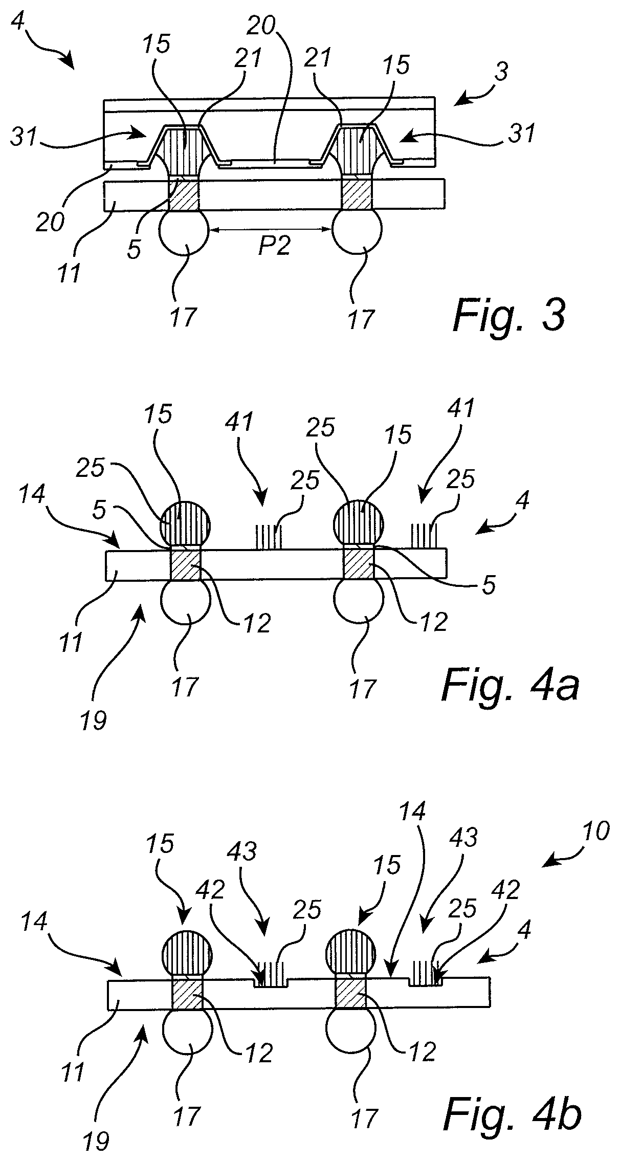
[0023]According to embodiments, the assembly platform may further comprise a second plurality of elongated nanostructures vertically grown on the first side of the assembly substrate. The second plurality of elongated nanostructures may be configured to other functions than the first plurality of nanostructures. The second plurality of nanostructures may be configured to dissipate heat from the IC to the assembly substrate thereby serving to improve thermal dissipation of e.g. an electronic assembly comprising the second plurality of elongated nanostructures. The second plurality of nanostructures may be configured to mechanically support the IC to thereby relieve stress on the nanostructure connection bumps exerted by e.g. the IC. The second plurality of nanostructures may be configured to reduce mismatch in coefficient of thermal expansion. Thus, the nanostructures flexes as a response to thermal expansion of e.g. the IC or substrate so that there is some degree of mismatch tolerance. The second plurality of nanostructures may be arranged as alignment marks or have optical functions (e.g. light absorbing black materials, frequency dependent / sensitive element). The second plurality of nanostructures may be arranged in a regular array to create structures to mimic artificial photonic crystals to function as optical interconnects or wave guides. To make a functional second plurality of nanostructures they may be designed to grown anywhere on the interposer according to embodiment design and functions.
[0030]According to an embodiment of the invention, the second plurality of nanostructures may be grown surrounding the at least one nanostructure connection bump. In other words, the second plurality of nanostructures may be arranged in around the periphery of the nanostructure connection bump. This way the second plurality of nanostructures may provide improved mechanical support between the assembly substrate and / or an IC.

Problems solved by technology

However, the potential of the today's conventional interposers faces the limitations on the number of devices that can be connected.
For example, the interposer may limit the form factor and / or the performance of a final electronic device since the number of components that can be interconnected is primarily limited by the interposer solder balls and its limitations in terms of size, pitch (a typical conventional pitch may be about 50 μm) and height.
The conventional interposers are relatively ‘unsmart’ which do not allow anything more than the interconnects and routing paths.
The I / O points or pillars made by the conventional technology also possess challenges to further miniaturize the I / O dimensions and increases the poor reliability issues and fatigue failures.
Accordingly, todays conventional interposers pose a limitation on the number devices that can be connected due to the arrangement of the solder balls or the metallic materials that creates the connection.
This may lead to that the interposer may limit the performance of a final electronic device since the number of components that can be interconnected is set by the interposer solder ball and its limitations.

Method used


Image

  • Assembly platform
  • Assembly platform
  • Assembly platform

Examples


Embodiment Construction

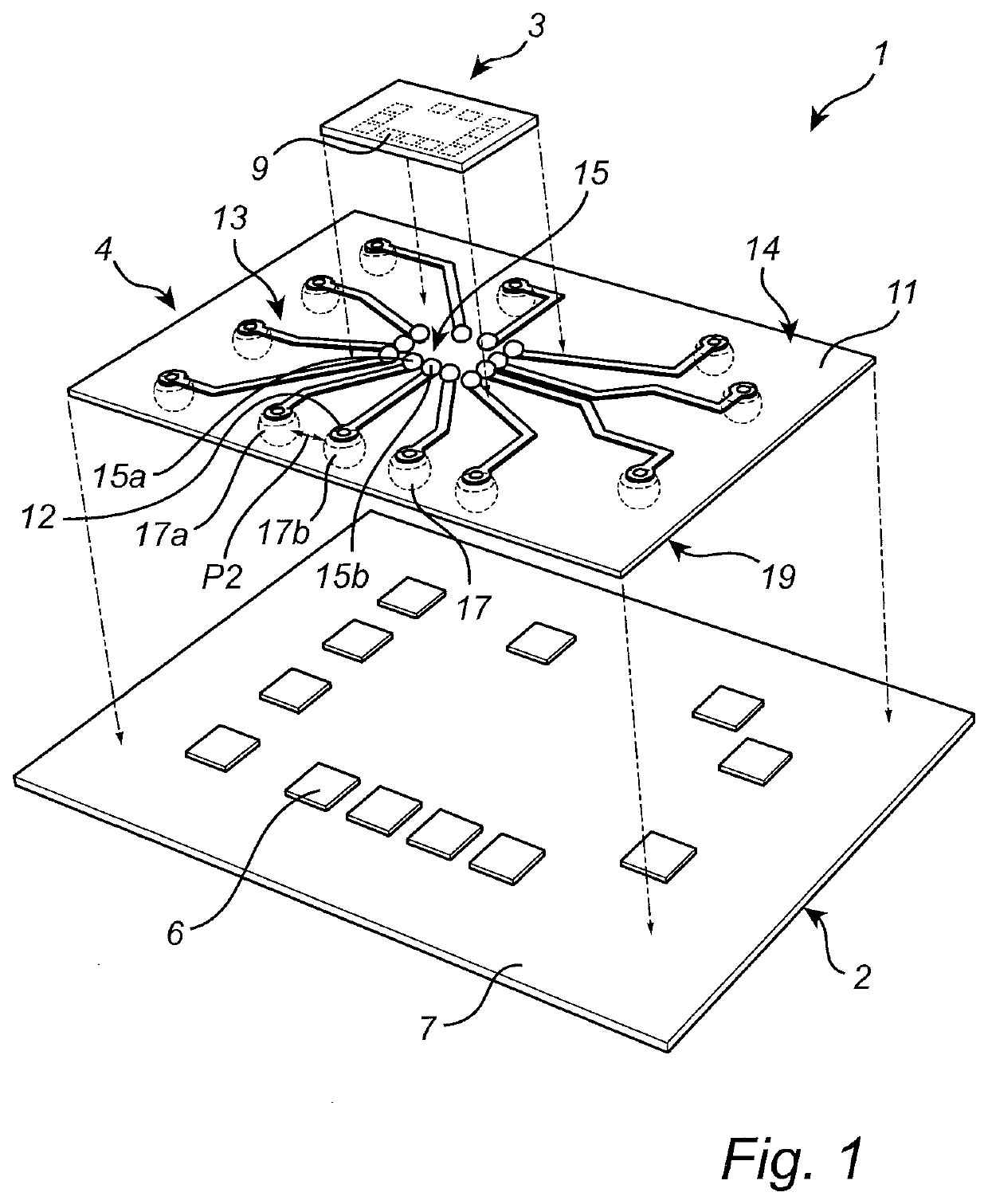
[0065]In the present detailed description, various embodiments of the assembly platform is mainly described with reference to an assembly platform being arranged as an interposer device between an integrated circuit and a substrate. However, it should be noted that this by no means limits the scope of the present invention, which equally well includes that the assembly platform may be arranged to interconnect any two types of electrical components, e.g. a die, silicon chips, integrated circuits, analog and / or digital circuits etc. Such an assembly platform may enable to have heterogeneous integration possibilities.

[0066]FIG. 1 schematically illustrates an electronic assembly 1 comprising a substrate, here in the form of a simplified printed circuit board (PCB) 2, an integrated circuit (IC) 3, and an assembly platform 4 arranaed as an interposer device according to an example embodiment of the present invention. The PCB includes PCB connection pads 6 formed on a PCB-substrate 7, and ...


PUM

PropertyMeasurementUnit
heightaaaaaaaaaa
thickaaaaaaaaaa
conductiveaaaaaaaaaa

Abstract

An assembly platform for arrangement as an interposer device between an integrated circuit and a substrate to interconnect the integrated circuit and the substrate through the assembly platform, the assembly platform comprising: an assembly substrate; a plurality of conducting vias extending through the assembly substrate; at least one nanostructure connection bump on a first side of the assembly substrate, the nanostructure connection bump being conductively connected to the vias and defining connection locations for connection with at least one of the integrated circuit and the substrate, wherein each of the nanostructure connection bumps comprises: a plurality of elongated conductive nanostructures vertically grown on the first side of the assembly substrate, wherein the plurality of elongated nanostructures are embedded in a metal for the connection with at least one of the integrated circuit and the substrate, at least one connection bump on a second side of the assembly substrate, the second side being opposite to the first side, the connection bump being conductively connected to the vias and defining connection locations for connection with at least one of the integrated circuit and the substrate.

Description

CROSS-REFERENCE TO RELATED APPLICATION[0001]This Application is a Section 371 National Stage Application of International Application No. PCT / SE2017 / 050430, filed May 3, 2017 and published as WO 2017 / 192096 on Nov. 9, 2017, in English, which claims the benefit of priority of Swedish Application No. 1630103-8, filed on May 6, 2016, the entire contents of which are hereby incorporated by reference in their entirety.FIELD OF THE INVENTION[0002]The present invention relates to an assembly platform for arrangement between an electronic device and a substrate to interconnect the first electronic device and the substrate through the assembly platform. The present invention also relates to a method of manufacturing such an assembly platform.BACKGROUND OF THE INVENTION[0003]In today's electronics, size and form factors are of significant consideration in any physical arrangement of chips. Due to the rapid progress in portable electronic devices the demand for more compact physical arrangemen...

Claims


Application Information

Patent Timeline
Patent Type & Authority Patents(United States)
IPC IPC(8): H01L23/00H01L21/48H01L23/31H01L23/498
CPCH01L23/49838H01L23/3128H01L23/49816H01L24/16H01L21/4853H01L23/49827H01L2224/10165H01L2224/16238H01L21/52H01L21/56H01L21/67121H01L21/768H01L23/31H01L23/498H01L23/50H01L23/528H01L24/14H01L24/17H01L24/97H01L29/0665
Inventor KABIR, M SHAFIQULJOHANSSON, ANDERSDESMARIS, VINCENTAMIN SALEEM, MUHAMMAD
Owner SMOLTEK AB
Learn More