Antenna devices to suppress ground plane interference

a technology of ground plane interference and antenna device, which is applied in the direction of antenna coupling, antenna details, antennas, etc., can solve the problems of limited bandwidth with small size, limited scanning range, etc., and achieves good spatial scanning, suppressing ground plane interference, and increasing total efficiency

Active Publication Date: 2020-11-17
FLORIDA INTERNATIONAL UNIVERSITY
View PDF3 Cites 17 Cited by
  • Summary
  • Abstract
  • Description
  • Claims
  • Application Information

AI Technical Summary

Benefits of technology

[0004]Embodiments of the subject invention provide novel and advantageous antenna devices that include a frequency selective surface (FSS) resistive card (R-card) to suppress ground plane interference. The antenna device can include a tightly coupled dipole array (TCDA), and the FSS R-card can be, for example, a saw-tooth ring (see FIG. 4) that only attenuates the intended frequencies, thereby increasing total efficiency. The antenna device can be an extremely wideband phased array with integrated feeding network and good spatial scanning (e.g., spatial scanning down to 60°). The antenna device can have a bandwidth of at least 50:1 (e.g., 58:1) together with the scanning capability down to 60° in both E- and H-planes, and the radiation efficiency can be at least 70% (e.g., at least 72% or at least 73%). The FSS R-card can provide an extremely wideband (EWB) impedance match.

Problems solved by technology

However, limitations still exist with respect to achieving wide bandwidth with small size and good scanning range.

Method used


Image

  • Antenna devices to suppress ground plane interference
  • Antenna devices to suppress ground plane interference
  • Antenna devices to suppress ground plane interference

Examples


example 1

[0058]An infinite array simulation was used to represent a 12×12 finite element array of the TCDA shown in FIGS. 1(a)-1(c) (FIG. 1(a) shows a 4×4 section of the 12×12 array) 1 using ANSYS HFSS v.19. The plane containing the direction of the current is denoted as the E plane, with the perpendicular plane denoted as the H plane. The infinite array VSWR for the principle planes, with scanning to 60° is shown versus frequency in FIG. 6. The array was designed for a VSWR<3 for 0.13 GHz to 6 GHz for an impedance bandwidth of 46:1 with scanning. A reduced performance in the low frequency H-plane VSWR is expected when scanning to low angles with dual-polarized planar arrays due to its 1 / cos(θ) free space impedance, hence the mismatch around 2 GHz at 60°. The array was characterized by its near theoretical gain and average principle plane polarization purity of 40 dB as shown in FIG. 7. The co- and cross-polarized gains of the unit cell for the D-plane, with scanning to 60°, are shown versus...

example 2

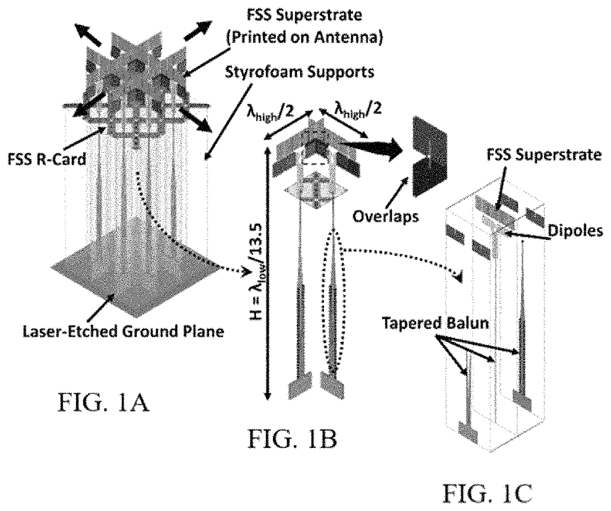
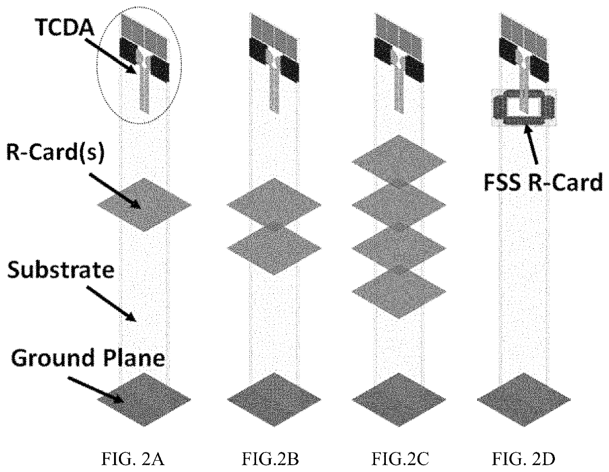
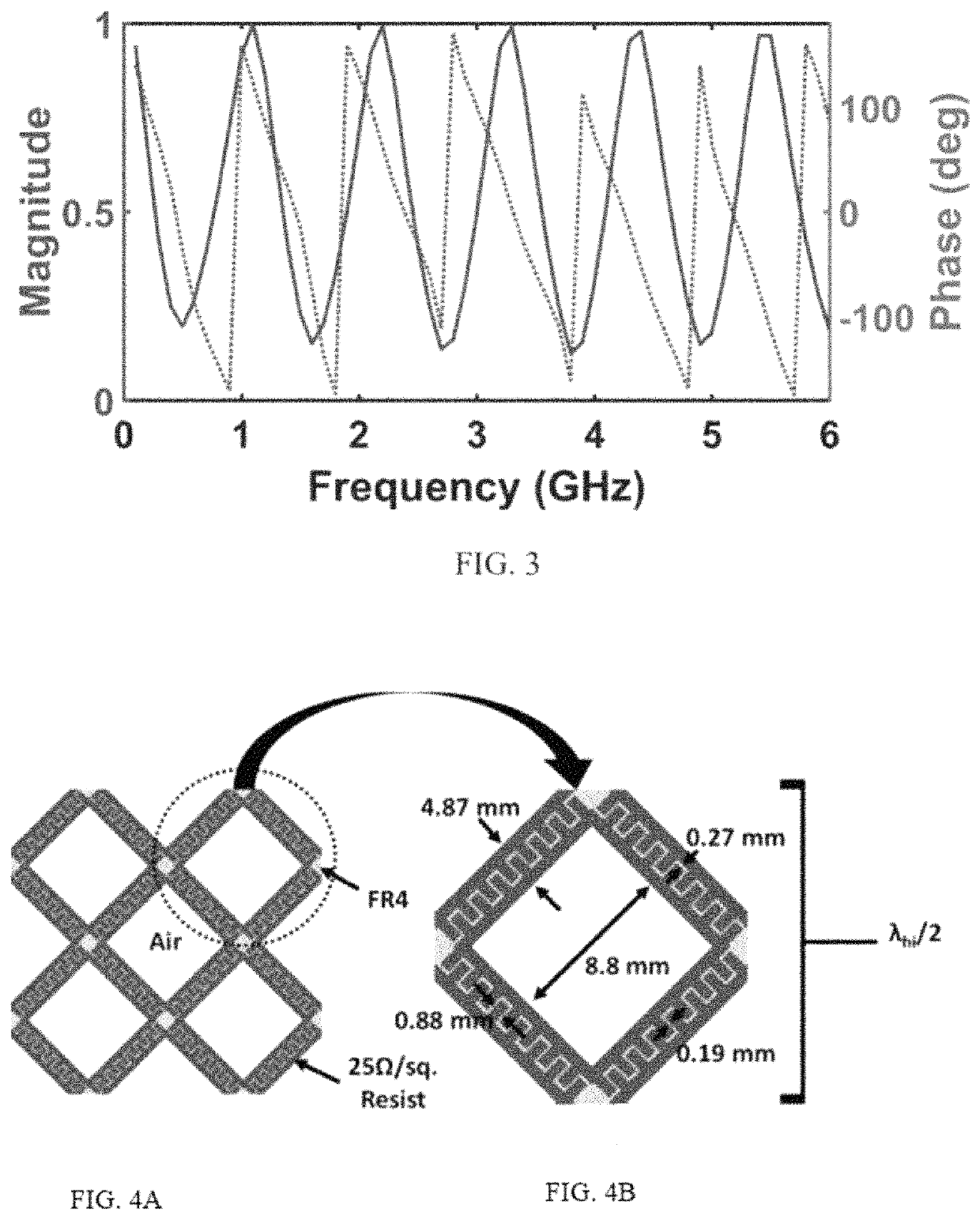
[0059]A 12×12 dual-polarized TDCA was fabricated and tested. The TDCA included an FSS R-card and is shown in FIGS. 9, 10(a), 10(b), 11, 12(a), 12(b), and 23-26. The FSS metal superstrate was printed on the vertical antenna cards for optimized scanning performance. The antenna board was constructed from two layers of 10 mil (1 mil=0.001 inches) thick Rogers 3003 with εr=3.0. The fabricated ground board was milled from a metalized 60 mil FR4 board with cutouts for securing the antenna cards. A total of four ground plane sections were joined together with copper tape to form a lightweight, structurally stable and resonance free ground plane for testing the array.

[0060]The tolerances of commercial PCB manufacturing were constantly considered in the design process, where metal thickness and via misalignment result in a significant change from the ideal design. The design used 10 mil diameter vias and a minimum metal tolerance of 0.1524 mm (6 mil) in accordance with standard low-cost comm...


PUM


Abstract

Antenna devices that include a frequency selective surface (FSS) resistive card (R-card) to suppress ground plane interference are provided. The antenna device can include a tightly coupled dipole array (TCDA), and the FSS R-card can be a saw-tooth ring that only attenuates the intended frequencies. The antenna device can be an extremely wideband phased array with integrated feeding network and spatial scanning down to 60°.

Description

BACKGROUND[0001]Low profile wideband antennas and arrays are key components in a number of advanced communications and electronic warfare (EW) systems. For these systems, an ultra-wideband (UWB) array replaces several narrowband systems for orders of magnitude savings in power, cost, and space. They also enable increased data rates and secure spread spectrum communications. In addition to being wideband, these arrays must be low profile and operate across a wide scanning range for comprehensive spatial coverage from their designated platforms.[0002]The most used UWB arrays are the connected and coupled arrays that have been considered since the early 2000s. A planar wideband connected slot array can have a 6-15 GHz design that can scan down to 60° in the H-plane and 80° in the E-plane. Similarly, a variation of the coupled dipole known as the planar ultra-wideband modular antenna (PUMA) array can have 6:1 impedance bandwidth with direct unbalanced 50Ω feeding.[0003]Among low profile...

Claims


Application Information

Patent Timeline
Patent Type & Authority Patents(United States)
IPC IPC(8): H01Q15/00H01Q1/52H01Q21/06H01Q5/25H01Q21/00
CPCH01Q21/062H01Q21/0075H01Q1/523H01Q15/0013H01Q5/25
Inventor JOHNSON, ALEXANDERZHONG, JINGNIALWAN, ELIASVOLAKIS, JOHN L.
Owner FLORIDA INTERNATIONAL UNIVERSITY
Why Eureka
Try Eureka