Microelectronic treatment system having treatment spray with controllable beam size

a microelectronic treatment and control beam technology, applied in the direction of cleaning process and apparatus, cleaning of flexible articles, cleaning using liquids, etc., can solve the problems of difficult to provide, cryogenic treatment, and less practical scanning nozzle in cryogenic tools

Active Publication Date: 2021-06-01
TEL EPION
View PDF59 Cites 3 Cited by
  • Summary
  • Abstract
  • Description
  • Claims
  • Application Information

AI Technical Summary

Benefits of technology

[0008]This invention discloses strategies to adjust the beam size of a flow from a nozzle into a more or less focused treatment beam in order to clean particles from a substrate. The strategies use chamber features and the adjustment of the chamber pressure of the vacuum environment to tune the treatment beam to form a more or less focused beam to increase the removal efficiency of particles.
[0009]It has been discovered that mounting the nozzle into an auxiliary chamber helps to shape the treatment spray and to provide a more well-defined treatment beam whose size and focus can be easily adjusted on demand. For example, adjusting the chamber pressure of the vacuum system easily and rapidly tunes the treatment beam size, e.g., to make it more focused or more diffuse on demand. This offers the benefit to increase the particle removal efficiency on the substrate as the beam can be tuned to optimize cleaning performance for different kinds of contamination.
[0010]Generally, the smaller, more focused treatment beams provide cleaning directly below the nozzle, whereas the more diffuse beams clean a larger annular region radially further outward relative to the footprint of the nozzle over the wafer. The smaller beam is created with higher chamber pressure (e.g., 19 Torr in some modes of practice), while the more diffuse beam results from using a lower chamber pressure (e.g., about 4 Torr in some embodiments). The smaller beam generally flows directly downward onto the wafer in substantial alignment with the z-axis. The smaller beam may be more desirable to remove smaller particles, to clean recesses such as trenches as such recesses are in line-of-sight communication with the nozzle, or to protect delicate features that might be more likely to be damaged by lateral or angled flows. The more diffuse beam tends to impact the wafer more laterally. The more diffuse beam may be more desirable to use where higher throughput is desired, where more robust features are present, or the like.
[0011]The performance of the present invention is counter to conventional wisdom. Conventional wisdom generally correlates lower chamber pressures with better cleaning performance. Using the shaped beam strategies of the invention, higher pressures allow better cleaning performance directly under the nozzle.
[0012]In the practice of the present invention, the chamber pressure can be adjusted to quickly focus and collimate the flow to improve cleaning. This adjustment occurs rapidly in real time within a process recipe. Tool shutdown and reconfiguration is not required. Pressure profiles can be used within a treatment to optimize beam energy for different kinds of particles. The adjustment is fast enough that the beam can be tuned on the same wafer, if desired, so that some portions are treated by a relatively smaller, more focused beam, while other portions are treated by a larger, more diffuse beam. As another option, different beam sizes can be used to treat common areas in a sequence, if desired.
[0013]This method provides an avenue to overcome limited particle removal efficiency especially at small particle sizes less than 100 nm and enhances the probability to attain the required directionality needed to dislodge particles from the substrate directly underneath the nozzle. Advantages of such a perpendicular, collimated aerosol flow path include cleaning of smaller particles (<100 nm) directly underneath the nozzle that would not be cleaned as easily in a similar timeframe by a more diffuse flow. Additionally, targeted cleaning of specific regions of the substrate may be practiced, since the spot cleaning profile of the collimated flow can be modified to a precise size. This method of cleaning can also remove particles embedded in patterns more effectively because of the improved line-of-sight.

Problems solved by technology

However, a scanning nozzle is less practical in a cryogenic tool, because a cryogenic rotary coupling has been difficult to provide in a practical manner.
A significant challenge is to use cryogenic treatments to remove smaller particles, e.g., contaminant particles having a size under about 100 nm.
Generally, smaller particles are harder to remove than larger particles.
Unwanted particle contamination on semiconductor substrates can negatively impact the device yield, hence the need to reduce particles at different stages of the semiconductor manufacturing process.

Method used


Image

  • Microelectronic treatment system having treatment spray with controllable beam size
  • Microelectronic treatment system having treatment spray with controllable beam size
  • Microelectronic treatment system having treatment spray with controllable beam size

Examples


example 1

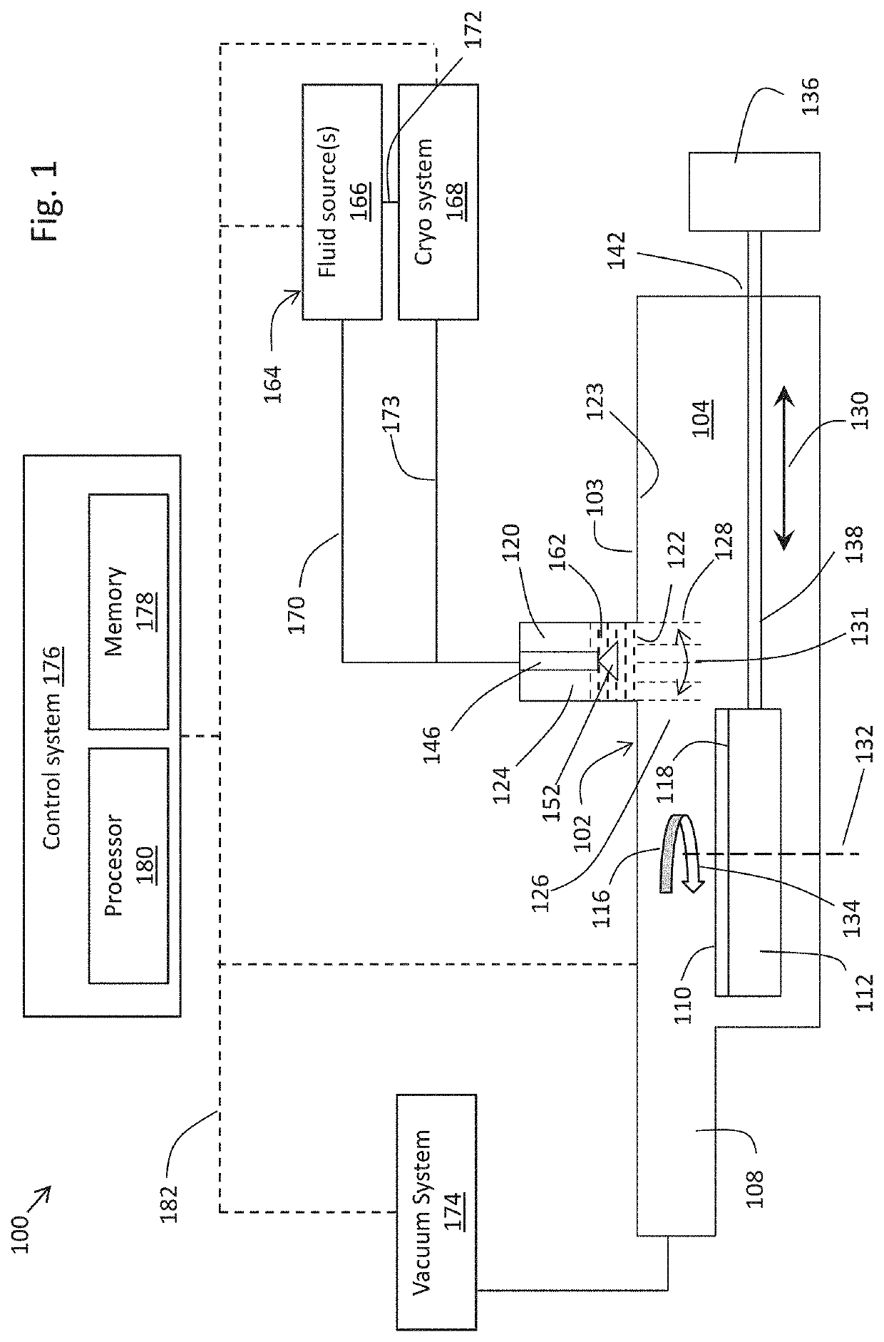
[0083]Referring to FIG. 5, tests (Tests 1 and 2) were conducted to demonstrate small particle cleaning of a 300 mm, bare silicon wafer 200 having a surface 201 contaminated with 30 nm silica particles and then exposed to cryogenic aerosol treatment beams at two different chamber pressures, respectively. A relatively more concentrated treatment beam at relative higher vacuum chamber pressure of 19 Torr was used for one test. This was compared to a larger, more diffuse treatment beam at lower chamber pressure of 4 Torr under otherwise the same conditions for a second test.

[0084]To prepare the wafer for testing, 30 nm silica particles were wet deposited onto the bare silicon wafer 200, aged for 3 hours, and then placed into a vacuum chamber in a cryogenic treatment tool according to FIG. 1 and FIG. 4. The tool was configured to have, the capability to control the chamber pressure. A nozzle was mounted in a cylindrical auxiliary chamber such that the nozzle orifice was 50 mm from the su...

example 2

[0092]Tests were conducted to evaluate how flow rate and chamber pressure impact the shape and size of fluid treatment beams used to clean particles from wafer surfaces. The tests were conducted using a 300 mm, bare silicon wafer having a surface contaminated with 30 nm silica particles. The contaminated wafer was exposed to fluid treatment beams in four different tests (Tests 3, 4, 5 and 6) using the conditions reported in Table 2-1.

[0093]To prepare each test wafer for testing, 30 nm silica particles were wet deposited onto the bare silicon wafer 200, aged for 1 hour, and then placed into a vacuum chamber in a cryogenic treatment tool according to FIG. 1 and FIG. 4. The tool was configured to have, the capability to control the chamber pressure. A nozzle was mounted in a cylindrical auxiliary chamber such that the nozzle orifice was 50 mm from the substrate. The nozzle orifice was 0.0925 inches (2.35 mm) in diameter. The nozzle also was recessed 27 mm within the cylindrical auxilia...

example 3

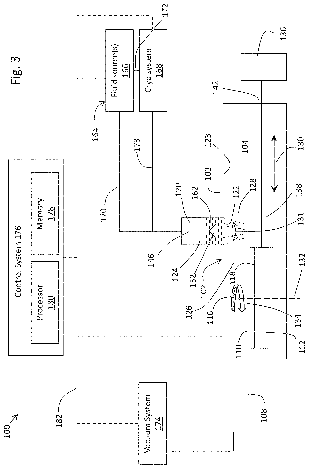
[0101]Tests were conducted to evaluate how flow rate, nozzle orifice size, and gap distance (shown as gap distance 126 in FIG. 4) impact the shape and size of fluid treatment beams used to clean particles from wafer surfaces. The tests were conducted using a 300 mm, bare silicon wafer having a surface contaminated with 100 nm silica particles. The contaminated wafer was exposed to fluid treatment beams in three different tests (Tests 7, 8 and 9) using the conditions reported in Table 3-1. For all three tests, pressurized and cooled argon was supplied to the nozzle −173 C (100 K) at the pre-expansion pressures shown in Table 3-1. The pressure and temperature were selected to help ensure that the pressurized and cooled argon supplied to the nozzle remained as a gas in the supply line to avoid liquid content. For all three tests, the nozzle was positioned with its outlet orifice outside the auxiliary chamber and projecting into the process chamber so that the nozzle outlet was not rece...


PUM


Abstract

This invention relates to systems and methods that produce a treatment beam with a controllable beam size. This is accomplished by providing an auxiliary chamber in open fluid communication with the main process chamber. A nozzle is mounted in a recessed manner in the auxiliary chamber. The nozzle dispenses a treatment spray into the auxiliary chamber. The auxiliary chamber shapes and dispenses the treatment material as a treatment beam into the process chamber. In illustrative embodiments, control of process chamber pressure adjusts the beam size of a treatment beam used to treat the surface of one or more microelectronic substrates.

Description

PRIORITY[0001]This application claims priority to U.S. Provisional Patent Application No. 62 / 632,131, filed Feb. 19, 2018, titled “Microelectronic Treatment System Having Treatment Spray with Controllable Beam Size,” the entire disclosure of which is incorporated herein by reference for all purposes.FIELD OF USE[0002]This disclosure relates to an apparatus and method for treating the surface of one or more microelectronic substrates, e.g., cleaning residue, debris, and other materials from a surface of a microelectronic substrate. More specifically, the disclosure relates to such an apparatus in which pressure is controlled to adjust the beam size of a treatment stream used to treat the surface of one or more microelectronic substrates.BACKGROUND OF THE INVENTION[0003]Advances in microelectronic technology cause integrated circuits (ICs) to be formed on substrates, such as semiconductor substrates, with ever increasing density of active components. The formation of ICs is carried ou...

Claims


Application Information

Patent Timeline
Patent Type & Authority Patents(United States)
IPC IPC(8): B08B3/02B08B11/00B08B5/04B08B5/02
CPCB08B3/02B08B5/02B08B5/04B08B11/00H01L21/67051H01L21/6776H01L21/68764
Inventor MBANASO, CHIMAOBI W.
Owner TEL EPION
Why Eureka
Try Eureka