TFT pixel threshold voltage compensation circuit using a variable capacitor

Active Publication Date: 2021-07-20
SHARP KK
View PDF3 Cites 1 Cited by
  • Summary
  • Abstract
  • Description
  • Claims
  • Application Information

AI Technical Summary

Benefits of technology

[0013]Embodiments of the present application relate to pixel circuits that have improved compensation performance by utilizing an additional compensation element in form of a variable capacitor (varactor). The use of the variable capacitor (varactor) results in enhanced compensation performance that otherwise may be degraded from a variety of sources. For example, after the compensation phase, switching activity of the switch transistors sk

Problems solved by technology

For example, after the compensation phase, switching activity of the switch transistors skews and degrades compensation performance.
Some pixel circuits have a short compensation time to run at higher frequencies, resulting in insufficient compensation performance.
Undesired parasitic capacitive coupling between voltage nodes also can result in degraded compensation performance.
The threshold co

Method used


Image

  • TFT pixel threshold voltage compensation circuit using a variable capacitor
  • TFT pixel threshold voltage compensation circuit using a variable capacitor
  • TFT pixel threshold voltage compensation circuit using a variable capacitor

Examples


first embodiment

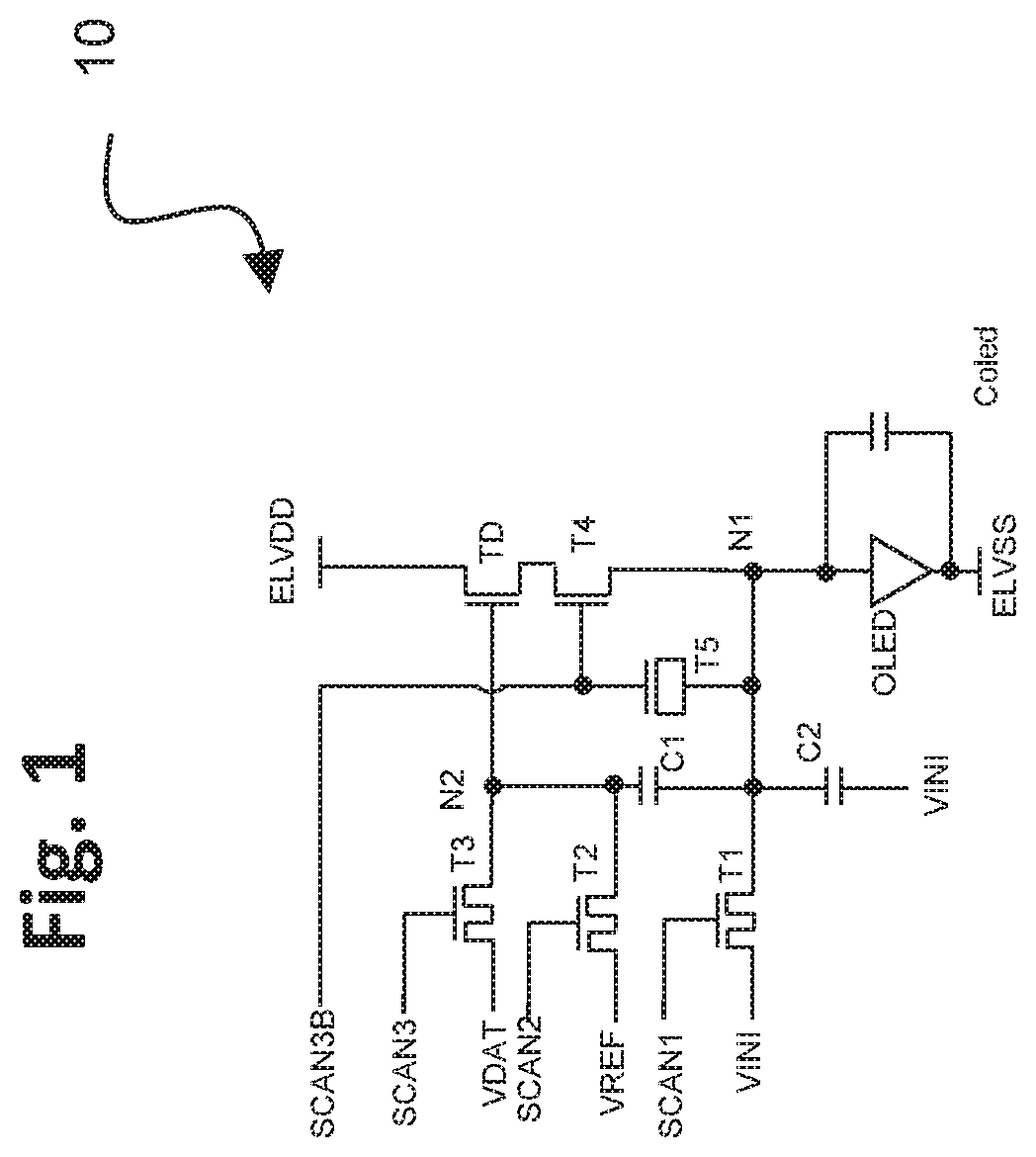
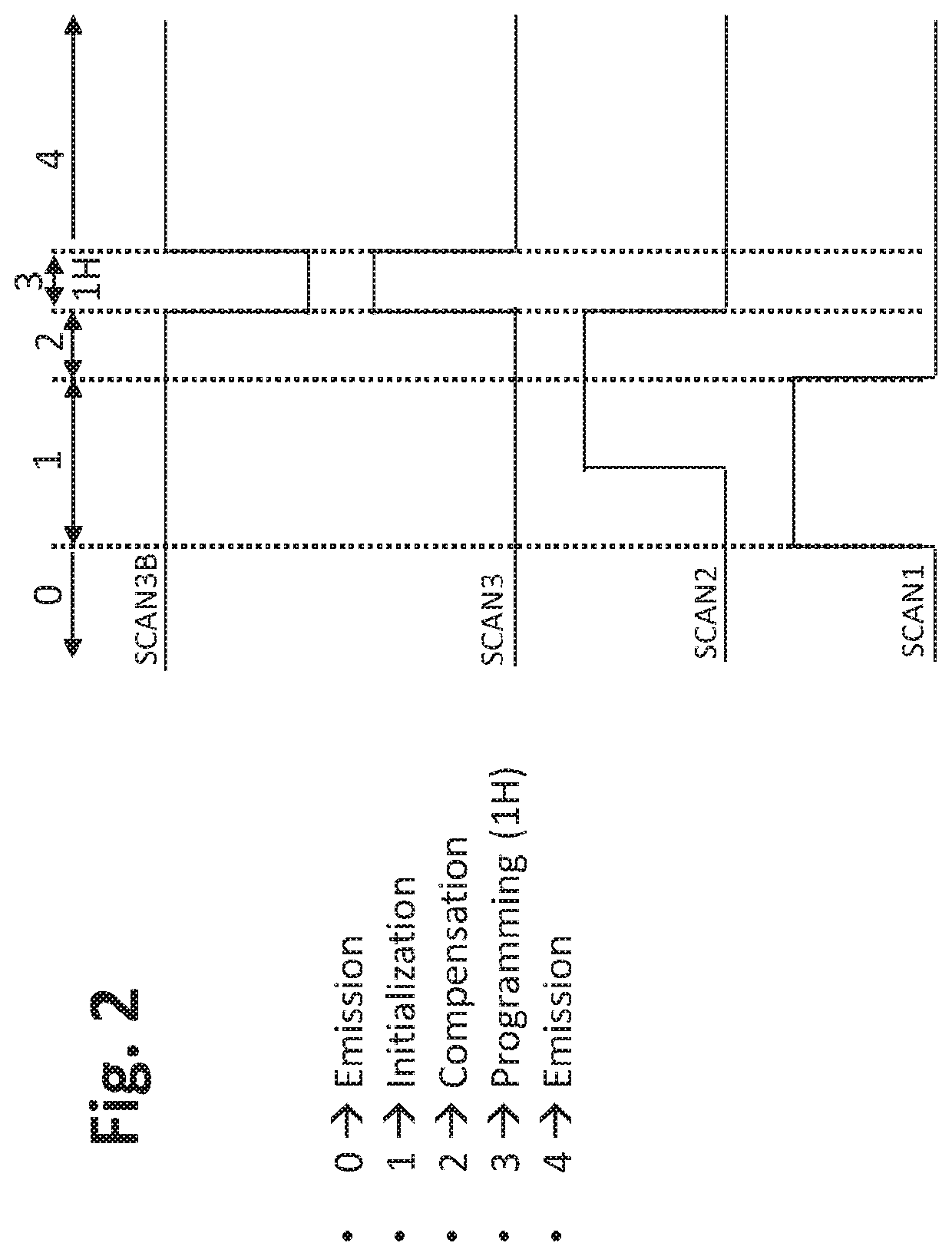
[0037]In this first embodiment, during the previous emission phase, the SCAN3B control signal has a high voltage level, so transistor T4 is on and the light-emitting device is electrically connected to the drive transistor. Light emission is being driven by the input driving voltage ELVDD connected to the drive transistor TD, whereby the actual current applied to the OLED is determined by the gate-source voltage of the drive transistor. Control signals SCAN1, SCAN2 and SCAN3 are at low voltage levels, and thus switch transistors T1, T2 and T3 are in the off state.

[0038]At the beginning of the initialization phase, the SCAN1 signal level is changed from a low voltage value to a high voltage value, causing switch transistor T1 to be switched to the on state. As transistor T1 is turned on, an initialization voltage VINI is applied from an initialization voltage supply line through T1 to the anode of the OLED. The initialization voltage VINI is set to lower than the threshold voltage of...

case a

[0060]

[0061]Δ⁢VN⁢1⁢α=Vν⁢α⁢r=-(CT⁢5⁢o⁢nC2+C1+CT⁢5⁢o⁢n⁢(VS⁢C⁢A⁢N⁢3⁢B⁢H-Vx)+CT⁢5⁢o⁢f⁢fC2+C1+CT⁢5⁢o⁢f⁢f⁢(Vx-VS⁢C⁢A⁢N⁢3⁢B⁢L))

case b

[0062]

[0063]Δ⁢VN⁢1⁢b=-(CT⁢5⁢o⁢nC2+C1+CT⁢5⁢o⁢n⁢(VS⁢C⁢A⁢N⁢3⁢B⁢H-(Vx-Δ⁢VT⁢H))+CT⁢5⁢o⁢f⁢fC2+C1+CT⁢5⁢o⁢f⁢f⁢((Vx-Δ⁢VT⁢H)-VS⁢C⁢A⁢N⁢3⁢B⁢L))

[0064]It follows:

[0065]Δ⁢Vv⁢a⁢r=Δ⁢VN⁢1⁢b-Δ⁢VN⁢1⁢a=-Δ⁢VT⁢H⁢CT⁢5⁢o⁢nC2+C1+CT⁢5⁢o⁢n+Δ⁢VT⁢H⁢CT⁢5⁢o⁢f⁢fC2+C1+CT⁢5⁢o⁢f⁢f⁢I⁢f⁢⁢C2+C1⪢CT⁢5⁢o⁢n⁢⁢and⁢⁢C2+C1⪢CT⁢5⁢o⁢f⁢f⁢⁢then⁢:⁢Δ⁢⁢Vv⁢a⁢r=Δ⁢VN⁢1⁢b-Δ⁢VN⁢1⁢a≈-(Δ⁢VT⁢H⁢CT⁢5⁢o⁢n-CT⁢5⁢o⁢f⁢fC2+C1)⁢Δ⁢⁢VN⁢1⁢b≈Vv⁢a⁢r+Δ⁢Vv⁢a⁢r

where CT5on is the gate capacitance of varactor T5 when a channel is formed,

where CT5off is the gate capacitance of varactor T5 when a channel is not formed,

where VSCAN3BH is the high voltage level of the signal SCAN3B,

where VSCAN3BL is the low voltage level of the signal SCAN3B,

where Vvar is the voltage change of N1 due to capacitive feedthrough of SCAN3B through T5, and

where ΔVvar is the excess voltage generated due to a threshold variation of the drive transistor TD.

[0066]When there is a threshold variation in the drive transistor TD, the varactor T5 will generate an excess voltage ΔVvar. The calculati...


PUM


Abstract

A pixel circuit for driving a light-emitting device for a display device is operable in an initialization phase, a compensation phase, a data programming phase, and an emission phase. The one horizontal time is minimized while maintaining accurate compensation of the threshold voltage of the drive transistor, and the pixel circuit further employs a varactor to compensate for variations in the threshold voltage of the drive transistor and for parasitic capacitances that arise within the pixel circuit. A capacitance of the varactor varies with a voltage at a node N1 constituting an electrical connection during the compensation phase of the drive transistor, the light-emitting device, a storage capacitor, and the varactor. The use of the capacitance variation of the varactor accounts for a variation in the threshold voltage of the drive transistor and for parasitic capacitances in the pixel circuit. The varactor may be implemented as a thin film transistor that operates as a variable capacitor.

Description

TECHNICAL FIELD[0001]The present invention relates to design and operation of electronic circuits for delivering electrical current to an element in a display device, such as for example to an organic light-emitting diode (OLED) in the pixel of an active matrix OLED (AMOLED) display device.BACKGROUND ART[0002]Organic light-emitting diodes (OLED) generate light by re-combination of electrons and holes, and emit light when a bias is applied between the anode and cathode such that an electrical current passes between them. The brightness of the light is related to the amount of the current. If there is no current, there will be no light emission, so OLED technology is a type of technology capable of absolute blacks and achieving almost “infinite” contrast ratio between pixels when used in display applications.[0003]Several approaches are taught in the prior art for pixel thin film transistor (TFT) circuits to deliver current to an element of a display device, such as for example an org...

Claims


Application Information

Patent Timeline
IPC IPC(8): G09G3/325G09G3/3283
CPCG09G3/325G09G3/3283G09G2320/0204G09G3/3233G09G2300/0819G09G2300/0852G09G2310/0251G09G2310/0262G09G2320/045
Inventor HEGANOVIC, ADNANLU, TONGBROWNLOW, MICHAEL JAMES
Owner SHARP KK
Why Eureka
Try Eureka