Semiconductor package and method of manufacturing the semiconductor package
- Summary
- Abstract
- Description
- Claims
- Application Information
AI Technical Summary
Benefits of technology
Problems solved by technology
Method used
Image

Examples
Embodiment Construction
[0023]Hereinafter, example embodiments will be explained in detail with reference to the accompanying drawings.
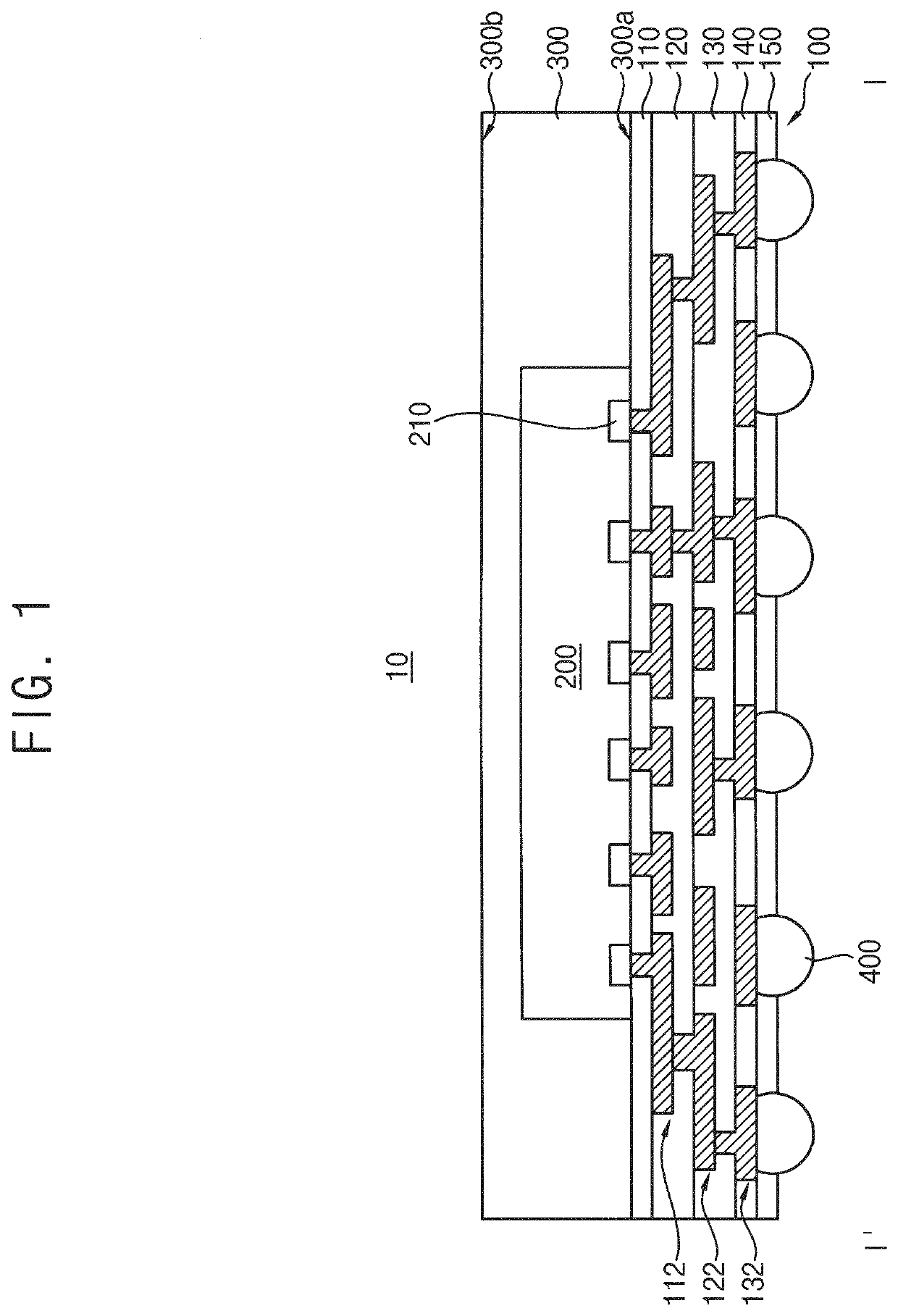
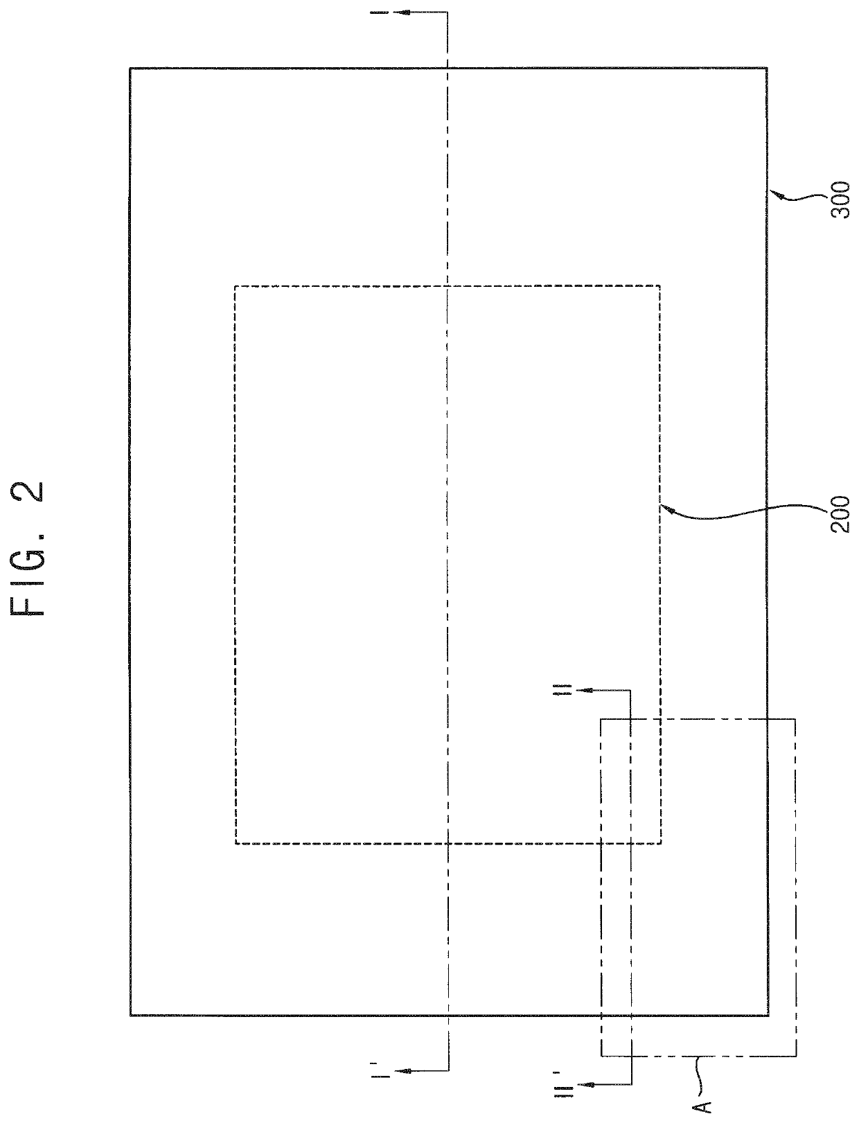
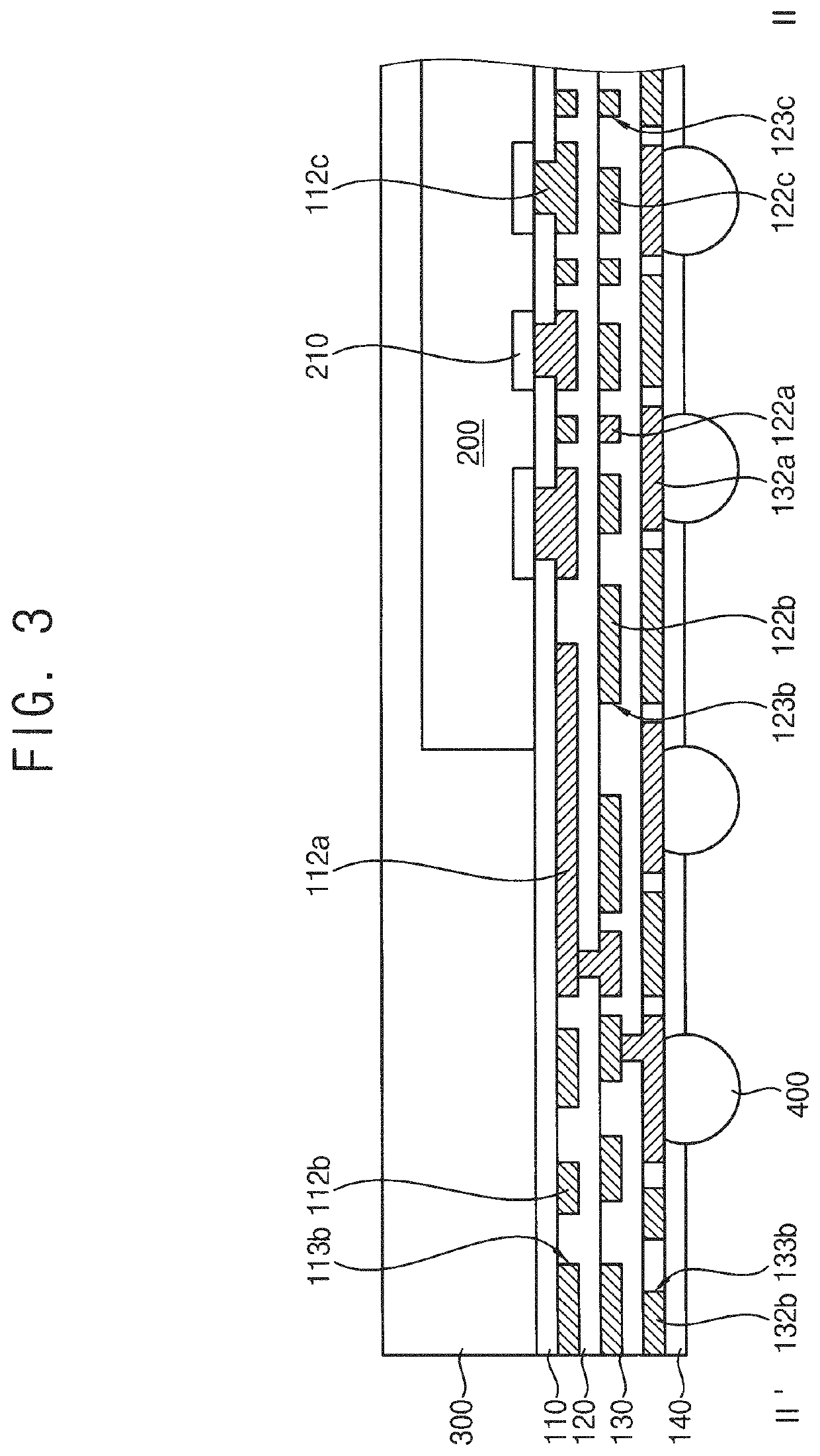
[0024]FIG. 1 is a cross-sectional view illustrating a semiconductor package in accordance with example embodiments. FIG. 2 is a plan view illustrating the semiconductor package in FIG. 1. FIG. 3 is a cross-sectional view taken along the line II-II′ in FIG. 2. FIGS. 4 and 5 are plan views illustrating a first redistribution wiring layer and a second redistribution wiring layer in regions overlapping with portion A in FIG. 2. FIG. 1 is a cross-sectional view taken along the line I-I′ in FIG. 1. FIG. 3 includes cross-sectional portions taken along the line II-II′ in FIGS. 4 and 5.
[0025]Referring to FIGS. 1 to 5, a semiconductor package 10 may include a mold substrate 300, a semiconductor chip 200 disposed in the mold substrate 300, and a redistribution wiring layer 100 covering a first surface 300a of the mold substrate 300 and including at least two redistribution wirings sta...
PUM
 Abstract
Description
Claims
Application Information