Temperature sensor element

a technology of temperature sensor and element, applied in the field of high temperature sensor element, can solve the problems of ceramic layer likely to crack, ceramic layer unlikely to crack, ceramic layer unlikely to crack, etc., and achieve the effect of preventing drift of resistance value or change of tcr

Active Publication Date: 2021-09-28
KOA CORP
View PDF24 Cites 0 Cited by
  • Summary
  • Abstract
  • Description
  • Claims
  • Application Information

AI Technical Summary

Benefits of technology

[0012]In the temperature sensor element configured thus, the protective film layer covering the platinum resistance pattern on the ceramic substrate includes: the trap layer as an inner layer that contains alumina as the main component and 2 to 30 vol % of platinum; and the overcoat layer as an outer layer that contains alumina as the main component. Accordingly, even when reactivity of the platinum resistance pattern becomes higher under high temperature use, platinum contained in the trap layer reacts with oxygen or impurities etc. contained in the ceramic substrate so that reaction of the platinum resistance pattern can be suppressed. Accordingly, it is possible to realize a highly reliable sensor in which drift of a resistance value or change of a TCR can be suppressed.
[0014]In the temperature sensor element configured thus, the surface smoothening layer containing alumina as the main component and 2 to 30 vol % of platinum is formed on the main surface of the ceramic substrate, and the protective film layer that is formed on the surface smoothening layer to cover the platinum resistance pattern includes the trap layer as an inner layer that contains alumina as the main component and 2 to 30 vol % of platinum, and the overcoat layer as an outer layer that contains alumina as the main component. Accordingly, even when reactivity of the platinum resistance pattern becomes higher under high temperature use, platinum contained in both the surface smoothening layer and the trap layer reacts with oxygen or impurities contained in the ceramic substrate so that reaction of the platinum resistance pattern can be suppressed. Particularly, reaction between the impurities contained in the ceramic substrate and the platinum resistance pattern can be suppressed due to the surface smoothening layer. Accordingly, it is possible to realize a highly reliable sensor in which drift of a resistance value or change of a TCR can be suppressed more greatly.
[0015]In the temperature sensor element having one of the aforementioned configurations, the trap layer has a two-layer structure including a lower layer and an upper layer; the lower layer is smaller in content of platinum than the upper layer and contains 0 to 10 vol % of platinum; and the upper layer contains 2 to 30 vol % of platinum. Since the lower layer is smaller in the content of platinum than the upper layer, the lower layer is sandwiched between the upper layer of the trap layer and the platinum resistance pattern, it is possible to increase the amount of platinum contained in the upper layer while using the lower layer to suppress change of the resistance value caused by platinum contained in the trap layer.
[0017]According to the temperature sensor element of the invention, it is possible to prevent drift of the resistance value or change of the TCR caused by reaction of the platinum resistance pattern or entry of the impurities into grain boundaries under high temperature use.

Problems solved by technology

However, in recent years, there is a demand for a sensor that can be used even at a high operating temperature exceeding 900° C. There arises a problem that the protective film layer covering the resistance pattern may be electrochemically decomposed in such a high temperature range.
Even when a continuous load is applied to the protective intermediate layer having the two-layer structure in a high temperature region, the ceramic layer is unlikely to crack while the ceramic paste layer is likely to crack.
Therefore, there is a problem that the impurities may cause drift of a resistance value or change of a TCR (Temperature Coefficient of Resistance).
Since the ceramic layer formed by the vapor deposition is in an amorphous state, it is impossible to use the ceramic layer to prevent the impurities from being diffused into the resistance pattern to suppress reaction of the impurities with platinum of the resistance pattern or entry of the impurities into the crystal grain boundaries of platinum.
In addition, when the alumina substrate is used as the ceramic substrate, it is impossible to suppress reaction of platinum of the resistance pattern with the impurities such as the sintering aid contained in the alumina substrate.
Accordingly, this also leads to the problem that the impurities may cause drift of the resistance value or change of the TCR.
In this case, there is however a problem that the platinum resistance pattern may be peeled from the sapphire substrate for reasons such as a large variation in linear expansion coefficient between platinum of the resistance pattern and the sapphire substrate, a decrease in adhesive strength of the resistance pattern to the sapphire substrate small in surface roughness, etc.

Method used


Image

  • Temperature sensor element
  • Temperature sensor element
  • Temperature sensor element

Examples


first embodiment

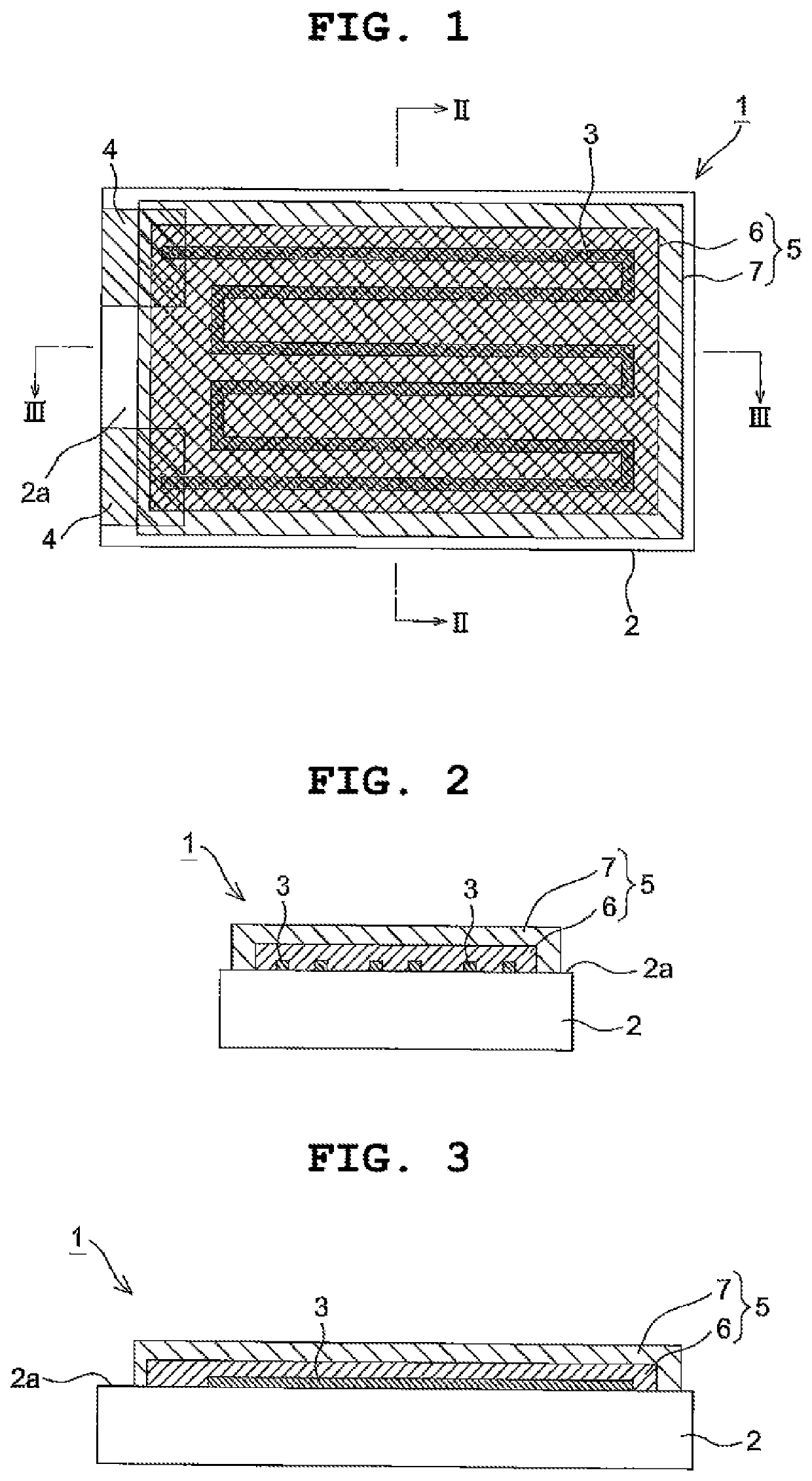
[0029]Embodiments of the invention will be described with reference to the drawings. Incidentally, in the following description, portions the same or regarded as the same in each of the embodiments will be referred to by the same signs correspondingly and respectively, and duplicated description thereof will be omitted appropriately. As shown in FIGS. 1 to 3, a temperature sensor element 1 according to a first embodiment of the invention is configured to include a ceramic substrate 2, a resistance pattern 3, a pair of electrodes 4, a protective film layer 5, and not-shown lead wires. The ceramic substrate 2 is shaped like a rectangular parallelepiped. The resistance pattern 3 having a meander shape is formed on a main surface (front surface) 2a of the ceramic substrate 2. The pair of electrodes 4 are formed on the main surface 2a of the ceramic substrate 2 so as to be connected to opposite end portions of the resistance pattern 3. The protective film layer 5 covers the resistance pa...

second embodiment

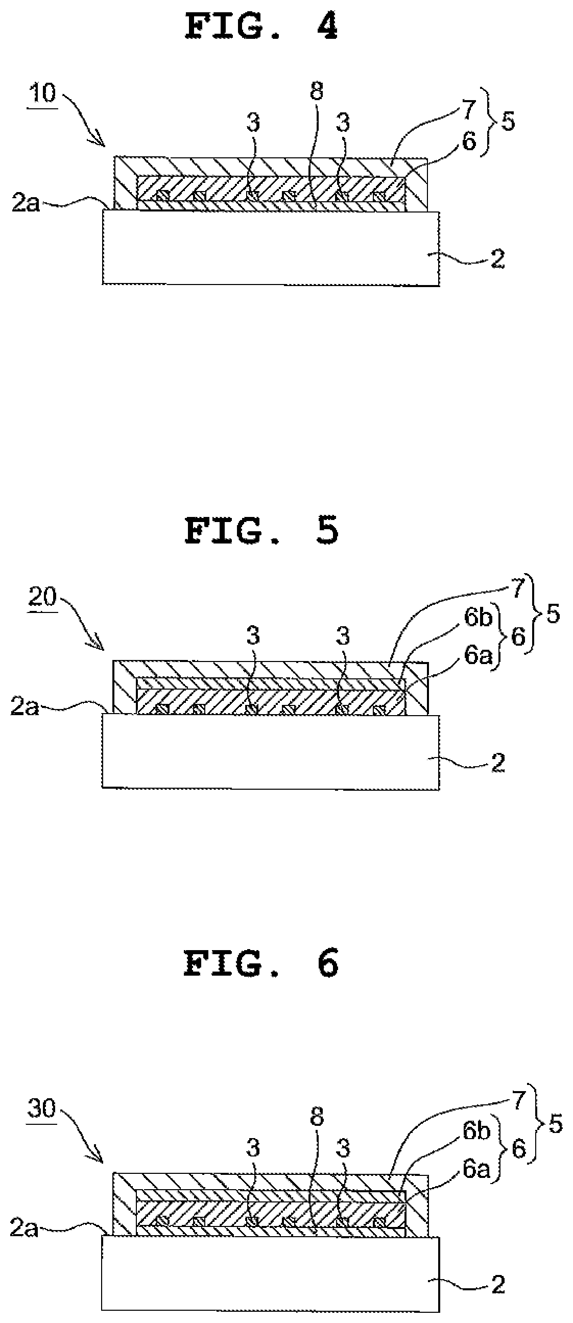
[0043]FIG. 4 is a sectional view of a temperature sensor element 10 according to a second embodiment of the invention. In FIG. 4, portions corresponding to those in FIG. 2 will be referred to by the same signs respectively.

[0044]The temperature sensor element 10 according to the second embodiment is basically the same in configuration as the temperature sensor element 1 according to the first embodiment except that a platinum resistance pattern 3 is not formed on a main surface 2a of a ceramic substrate 2 but a surface smoothening layer 8 containing alumina as a main component and 2 to 30 vol % of platinum is sandwiched between the platinum resistance pattern 3 and the main surface 2a of the ceramic substrate 2.

[0045]That is, in the temperature sensor element 10 shown in FIG. 4, the surface smoothening layer 8 containing alumina as the main component and platinum (whose content is 2 to 30 vol %) is formed on the main surface 2a of the ceramic substrate 2, and the resistance pattern ...

third embodiment

[0047]FIG. 5 is a sectional view of a temperature sensor element 20 according to a third embodiment of the invention. In FIG. 5, portions corresponding to those in FIG. 2 will be referred to by the same signs respectively.

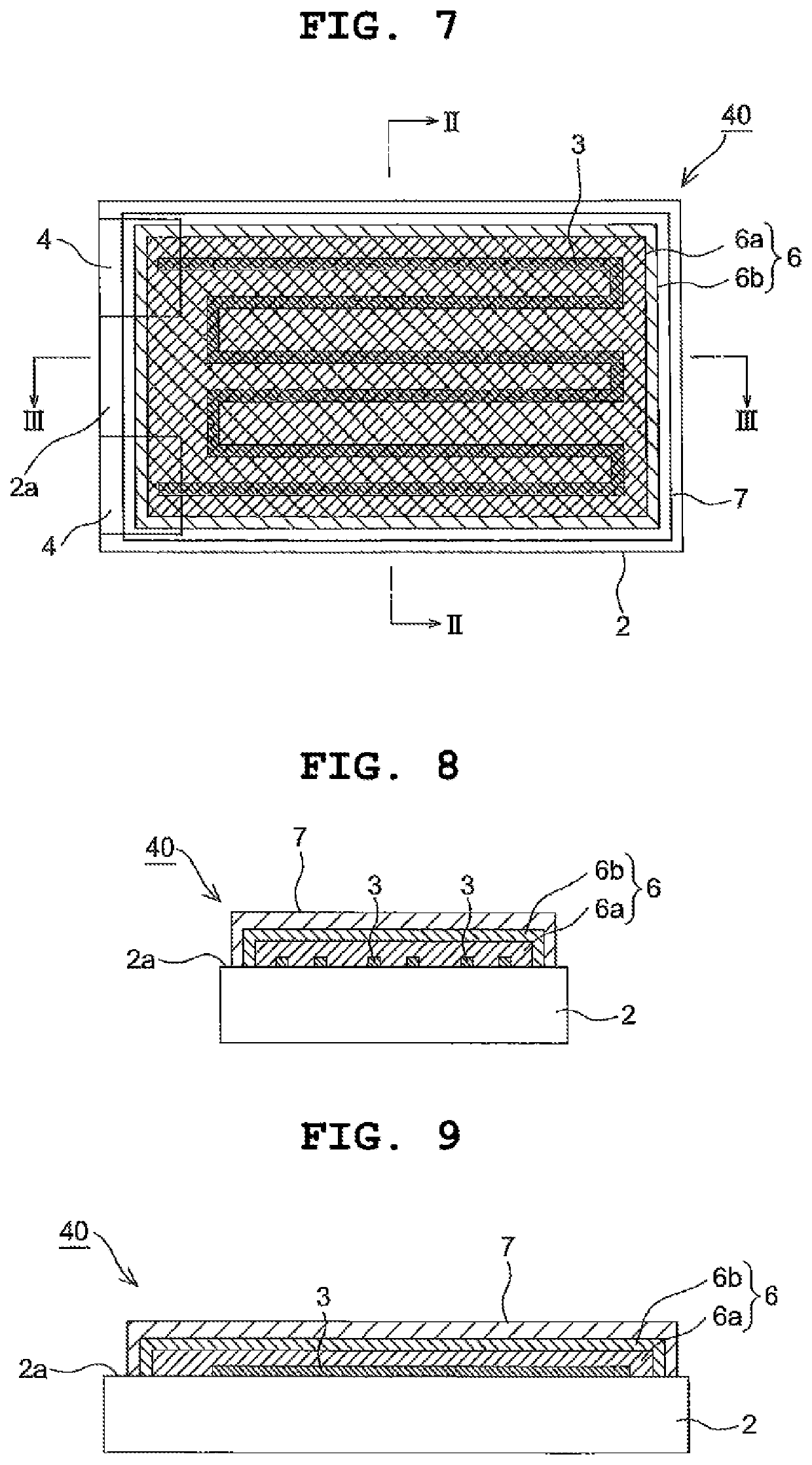
[0048]The temperature sensor element 20 according to the third embodiment is basically the same in configuration as the temperature sensor element 1 according to the first embodiment except that, of an overcoat layer 7 and a trap layer 6 constituting a protective film layer 5, the trap layer 6 is formed into a two-layer structure including a lower layer 6a and an upper layer 6b. Here, alumina is used as a main component in both the lower layer 6a and the upper layer 6b. The lower layer 6a making contact with the platinum resistance pattern 3 is smaller in content of platinum than the upper layer 6b and contains 0 to 10 vol % of platinum. The upper layer 6b contains 2 to 30 vol % of platinum. That is, when, for example, the content of platinum in the lower layer 6a ...


PUM

PropertyMeasurementUnit
operating temperatureaaaaaaaaaa
temperatureaaaaaaaaaa

Abstract

A resistance pattern that contains platinum as a main component is formed into a meander shape and on a main surface of a ceramic substrate. A protective film layer that covers the resistance pattern has a two-layer structure including a trap layer as an inner layer and an overcoat layer as an outer layer. The trap layer contains alumina as a main component and 2 to 30 vol % of platinum. The overcoat layer contains alumina as a main component. With such a configuration, even when reactivity of the platinum resistance pattern becomes higher under high temperature use, platinum contained in the trap layer reacts with oxygen or impurities etc. contained in the ceramic substrate. Thus, reaction of the platinum resistance pattern can be suppressed.

Description

BACKGROUND OF THE INVENTION1. Field of the Invention[0001]The present invention relates to a high temperature sensor element that is, for example, used for measurement of temperature of exhaust gas or a catalyst passing through an exhaust pipe of a car. Particularly, it relates to a temperature sensor element in which a resistance pattern containing platinum as a main component is formed on a ceramic substrate.2. Description of the Background Art[0002]A temperature sensor is attached to an exhaust pipe or a catalyst of a car. Temperature of exhaust gas is sent as an electric signal to an engine control unit (ECU). Combustion is controlled in accordance with the electric signal sent to the ECU so that, for example, protection of any component having strict heat-resistant restriction or temperature of the catalyst can be most suitable. As a result, the exhaust gas can be purified or fuel efficiency can be improved.[0003]As described in JP-A-11-121207, a flat plate type temperature sen...

Claims


Application Information

Patent Timeline
Patent Type & Authority Patents(United States)
IPC IPC(8): G01K7/18G01K1/10G01K1/08G01N27/407G01N27/12
CPCG01K1/10G01K1/08G01K7/18G01K7/183G01K2205/04G01N27/12G01N27/407G01N27/4071G01N27/4075G01N27/4077
Inventor MIURA, KATSUYASHIMODAIRA, MASAHIRO
Owner KOA CORP
Why Eureka
Try Eureka