

Photoelectric conversion element and solid-state imaging device
a conversion element and imaging device technology, applied in semiconductor devices, photovoltaic energy generation, solid-state devices, etc., can solve the problems of inability to obtain sufficient external quantum efficiency, easy delay of electric output signal with respect to incident light,
- Summary
- Abstract
- Description
- Claims
- Application Information
AI Technical Summary
Benefits of technology
Problems solved by technology
Method used
Image

Examples
embodiment
1. EMBODIMENT
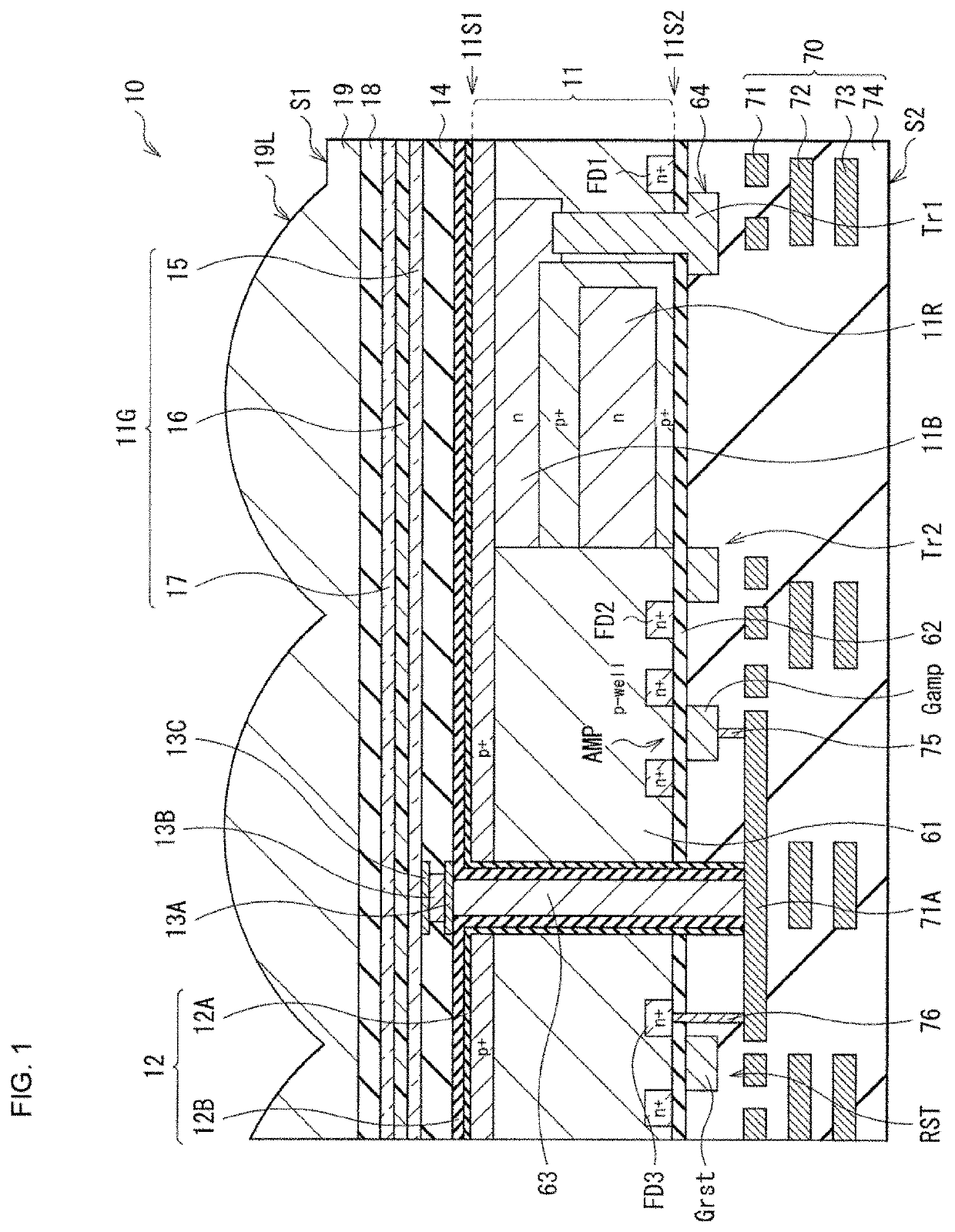
[0033]FIG. 1 illustrates a cross-sectional configuration of a photoelectric conversion element (photoelectric conversion element 10) according to an embodiment of the present disclosure. The photoelectric conversion element 10 is included, for example, in one pixel (unit pixel P) in a solid-state imaging device (solid-state imaging device 1) such as a backside illumination type (backside light receiving type) CCD (Charge Coupled Device) image sensor or CMOS (Complementary Metal Oxide Semiconductor) image sensor (see FIG. 8). The photoelectric conversion element 10 is of a so-called vertical spectroscopic type in which one organic photoelectric conversion section 11G, and two inorganic photoelectric conversion sections 11B and 11R are stacked in a vertical direction. The organic photoelectric conversion section 11G, and the two inorganic photoelectric conversion sections 11B and 11R each selectively detect respective pieces of light in different wavelength regions to per...
modification example
2. MODIFICATION EXAMPLE
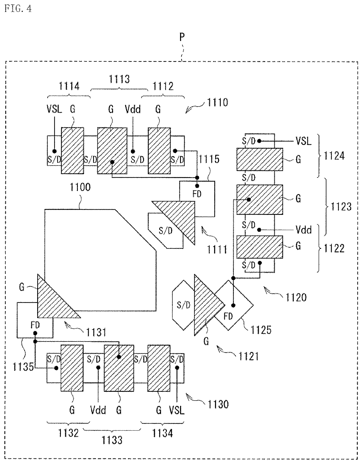
[0104]FIG. 7 illustrates a cross-sectional configuration of a photoelectric conversion element (photoelectric conversion element 20) according to a modification example of the present disclosure. The photoelectric conversion element 20 is included, for example, in one unit pixel P in the solid-state imaging element (solid-state imaging device 1) such as a backside illumination type CCD image sensor or CMOS image sensor, similarly to the photoelectric conversion element 10 according to the above-described embodiment, etc. The photoelectric conversion element 20 according to the present modification example has a configuration in which a red photoelectric conversion section 40R, a green photoelectric conversion section 40G, and a blue photoelectric conversion section 40B are stacked in this order on a silicon substrate 81 with the insulating layer 82 interposed therebetween.
[0105]The red photoelectric conversion section 40R, the green photoelectric conversion se...
application examples
3. APPLICATION EXAMPLES
Application Example 1
[0120]FIG. 8 illustrates, for example, an overall configuration of the solid-state imaging device 1 including the photoelectric conversion element 10 described in the above-described embodiment for each pixel. This solid-state imaging device 1 is a CMOS image sensor. The solid-state imaging device 1 includes, on the semiconductor substrate 11, the pixel section 1a as an imaging area, and a peripheral circuit unit 130 in a peripheral region of this pixel section 1a. The peripheral circuit unit 130 includes, for example, a row scanning section 131, a horizontal selection section 133, a column scanning section 134, and a system control section 132.
[0121]The pixel section 1a includes, for example, a plurality of unit pixels P (corresponding to, for example, the photoelectric conversion elements 10) that are two-dimensionally disposed in matrix. In these unit pixels P, pixel drive lines Lread (specifically, row selection lines and reset control...
PUM
| Property | Measurement | Unit |
|---|---|---|
| length | aaaaa | aaaaa |
| angle | aaaaa | aaaaa |
| angle | aaaaa | aaaaa |
Abstract
Description
Claims
Application Information