Capacitive compensation for vertical interconnect accesses

a technology of vertical interconnection and compensation, applied in the direction of high frequency circuit adaptation, impedence measurement, printed element electric connection formation, etc., can solve the problems of increased operating frequency, increased power consumption per operation of the resulting circuit, and signal loss

Active Publication Date: 2022-05-03
ACHRONIX SEMICON CORP
View PDF7 Cites 3 Cited by
  • Summary
  • Abstract
  • Description
  • Claims
  • Application Information

AI Technical Summary

Problems solved by technology

Discontinuities in electrical connections, including discontinuities resulting from VIAs, result in signal loss when the operating frequency increases.
Circuit designers compensate for this increased impedance by reducing the operating frequency or increasing the operating voltage, either of which increases the power consumption per operation of the resulting circuit.
An impedance discontinuity on the conductive path between the silicon die and the external balls leads to reflections and resonances, which hampers the transmitted signal in reaching the receiver.
However, the vertical VIA section introduces impedance discontinuities that can significantly affect signal integrity in high speed designs if the impedance transition from trace to VIA is too abrupt.
However, the first design has a loss spike at around 3 GHz, possibly due to a resonance.

Method used


Image

  • Capacitive compensation for vertical interconnect accesses
  • Capacitive compensation for vertical interconnect accesses
  • Capacitive compensation for vertical interconnect accesses

Examples


examples

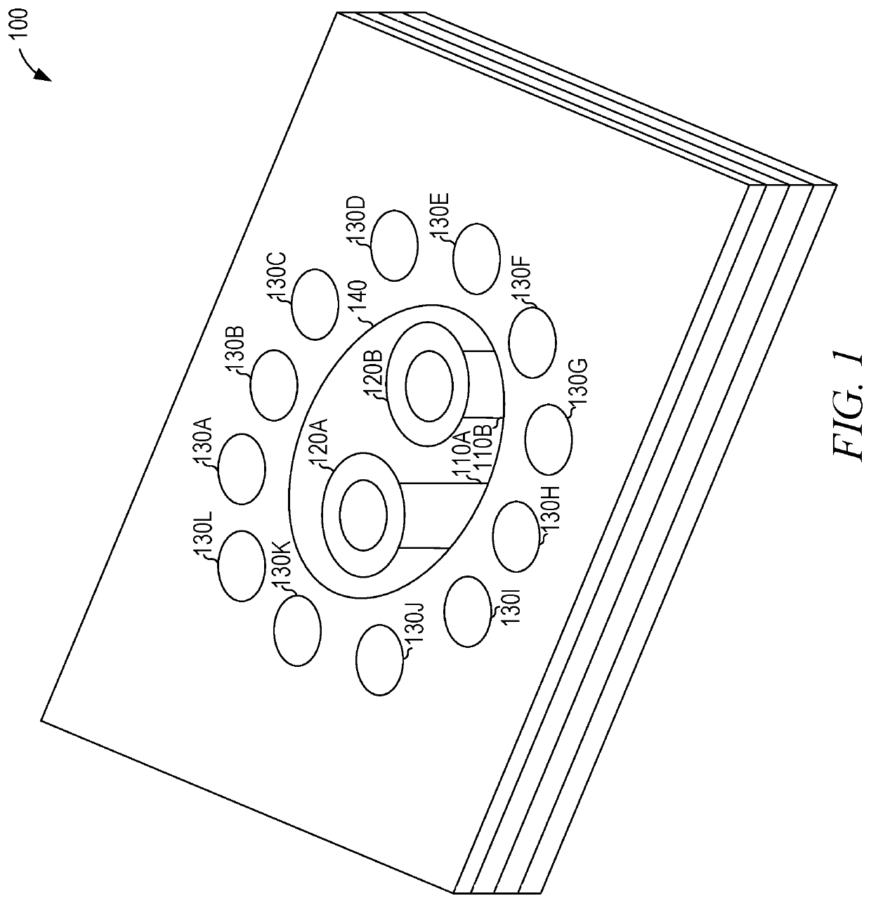
[0067]Example 1 is a multi-layer circuit comprising: a first circuit layer; a second circuit layer; a third circuit layer between the first circuit layer and the second circuit layer; a differential vertical interconnect access (VIA) connecting the first circuit layer and the second circuit layer, the differential VIA comprising at least two conductive elements for conducting a differential signal between the first circuit layer and the second circuit layer, the at least two conductive elements being surrounded by a single non-conductive region on the first circuit layer and the second circuit layer, the at least two conductive elements being surrounded by separate non-conductive regions on the third circuit layer.

[0068]In Example 2, the subject matter of Example 1 includes, wherein: the differential VIA comprises: a first VIA pad on the first circuit layer; and a second VIA pad on the second circuit layer; and the differential VIA lacks a VIA pad on the third circuit layer.

[0069]In...


PUM

PropertyMeasurementUnit
impedancesaaaaaaaaaa
peak impedanceaaaaaaaaaa

Abstract

Multiple designs for a multi-layer circuit may be simulated to determine impedance profiles of each design, allowing a circuit designer to select a design based on the impedance profiles. One feature that can be modified is the structure surrounding the barrels of a differential VIA on layers that are not connected to the differential VIA. Specifically, one antipad can be used that surrounds both barrels or two antipads can be used, with one antipad for each barrel. Additionally, the size of the antipad or antipads can be modified. These modifications affect the impedance of the differential VIA. Additionally, a conductive region may be placed that connects to the VIA barrel even though the circuit on the layer does not connect to the VIA. This unused pad, surrounded by a non-conductive region, also affects the impedance of the differential VIA.

Description

BACKGROUND[0001]Multi-layer circuits use vertical interconnect accesses (VIAs) to communicate electrical signals between layers. A VIA typically comprises a conductive barrel that connects two layers and passes through any intervening layers. After the layers of the multi-layer circuit are printed (e.g., by etching), holes are drilled through the layers and the conductive barrel is placed in the hole. During printing, conductive traces connect to the location that the barrel will be placed on layers connecting to the VIA. On other layers, a cylindrical clearing around the vias is created which provides insulation between the VIA and the metal on that layer. The conductive region surrounding a VIA on a connected layer is referred to as a pad; the non-conductive region surrounding a VIA on a layer, whether connected or unconnected, is referred to as an antipad. The holes may be plated with a conductive material (e.g., copper) that electrically connects the pads.[0002]Discontinuities i...

Claims


Application Information

Patent Timeline
Patent Type & Authority Patents(United States)
IPC IPC(8): H05K3/40H05K1/11H05K1/02G01R27/16H05K3/46H05K3/04H05K3/00H05K3/42
CPCH05K1/115G01R27/16H05K1/0245H05K1/0251H05K1/0298H05K1/116H05K3/0002H05K3/046H05K3/4038H05K3/429H05K3/46H05K2203/16Y10T29/49165H05K3/4611H05K3/4602H05K1/0221H05K2201/09636H05K2201/096
Inventor DSILVA, HANSEL DESMONDJ, SASIKALAJAIN, ABHISHEKKUMAR, AMIT
Owner ACHRONIX SEMICON CORP
Why Eureka
Try Eureka