Method for manufacturing a CMOS device

a manufacturing method and technology of cmos, applied in the direction of semiconductor devices, electrical devices, transistors, etc., can solve the problems of undesirable footing phenomenon, photoresist denaturation, and photoresist undercut at the bottom of the photoresist pattern

Active Publication Date: 2022-07-26
SHANGHAI HUALI INTEGRATED CIRCUIT CORP
View PDF15 Cites 0 Cited by
  • Summary
  • Abstract
  • Description
  • Claims
  • Application Information

AI Technical Summary

Benefits of technology

[0056]In summary, the embodiments of the present disclosure solve the problem of photoresist undercut after the silicon nitride sidewalls are formed, and avoid footing and ensure accurate patterns of the ion implantation regions by forming the shallow trench isolation, the gate structure, and the silicon nitride gate sidewalls, ALD depositing the silicon nitride film, to the gate structure, silicon nitride gate sidewalls and necessary device surface. This improvement is done without increasing lots of cost and complexity of the process.

Problems solved by technology

However, photoresists applied in dozens of photolithography processes in making ICs are sensitive to nitrogen-containing materials.
Thus, silicon nitride materials easily cause photoresist denaturation which generates an undesirable footing phenomenon.
However, at the 45 / 40 nm and below technology nodes, due to light reflection from the gate active region and the shallow trench isolation region, the current interface treatment performed by oxygen plasma is prone to creating the problem of photoresist undercut at the bottom of the photoresist patterns.
Thus, resultant pattern distortions affect regions defined by a number of ion implantation processes, such as lightly doped drain (LDD), halogen ion implantation, and source / drain (S / D) ion implantation, thereby impacting device performance.

Method used


Image

  • Method for manufacturing a CMOS device
  • Method for manufacturing a CMOS device
  • Method for manufacturing a CMOS device

Examples


Embodiment Construction

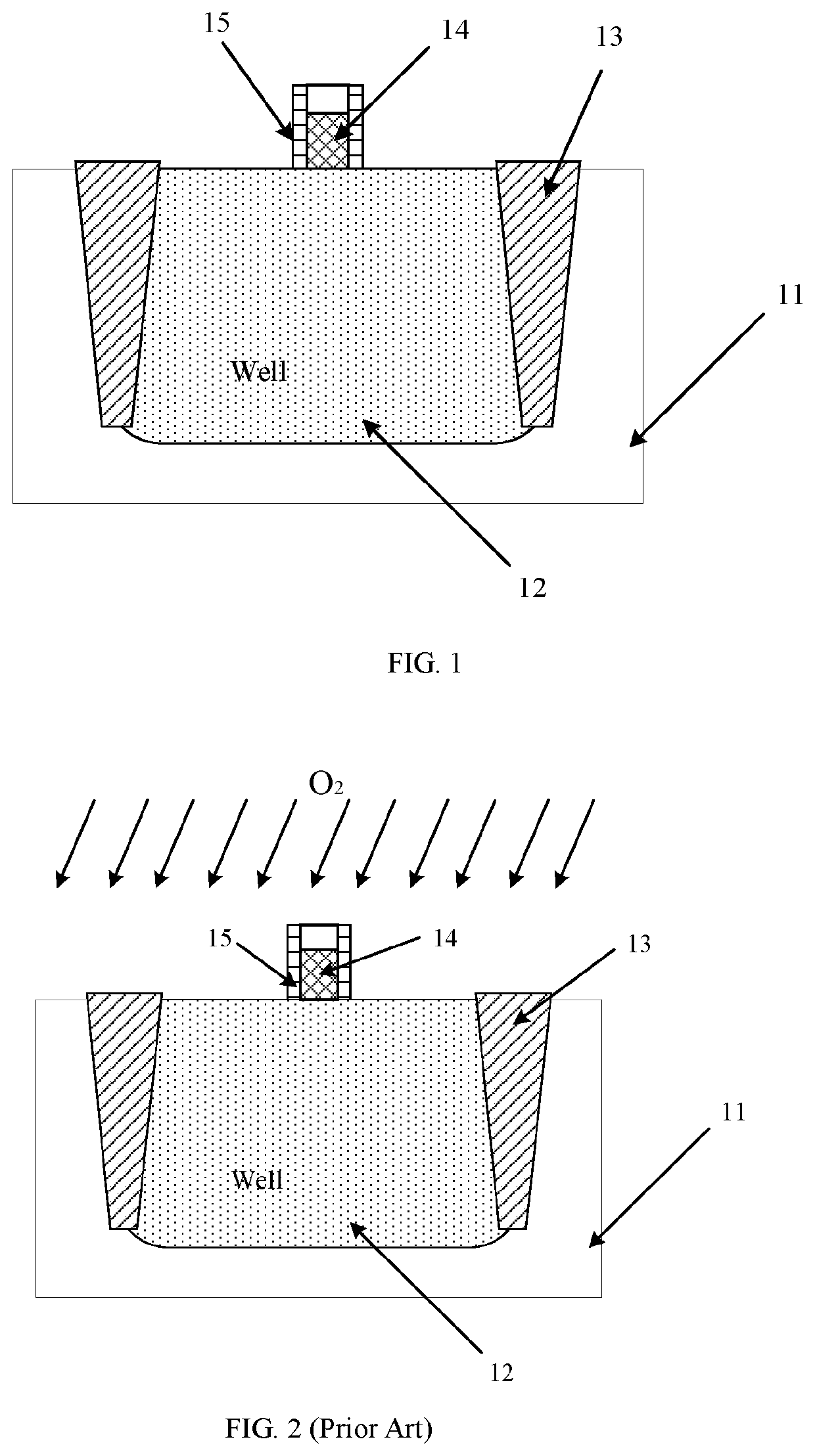
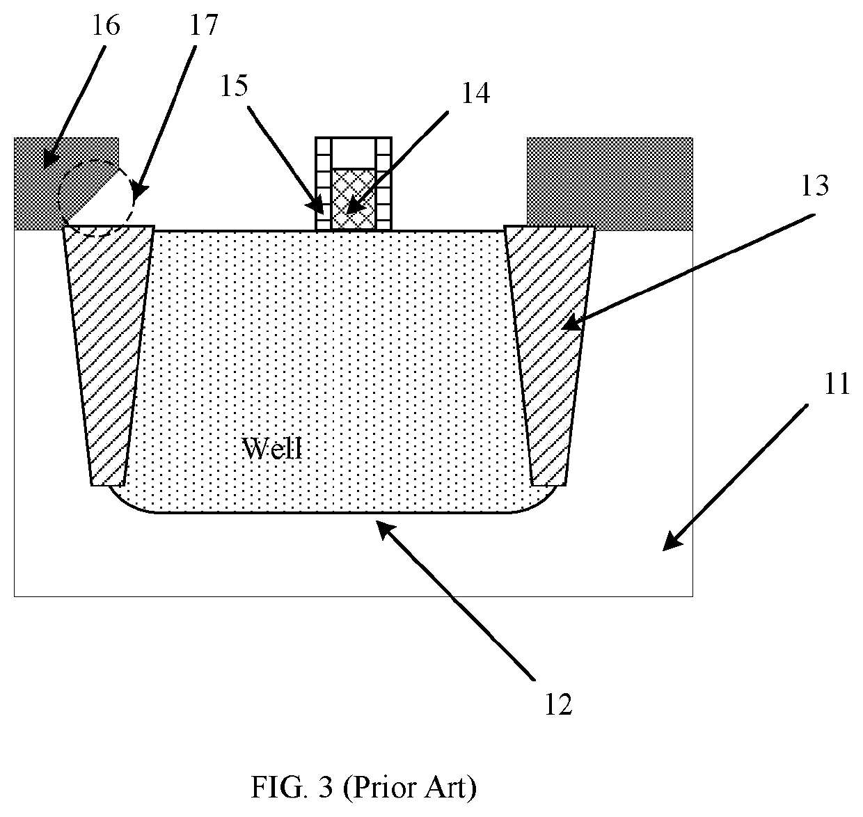
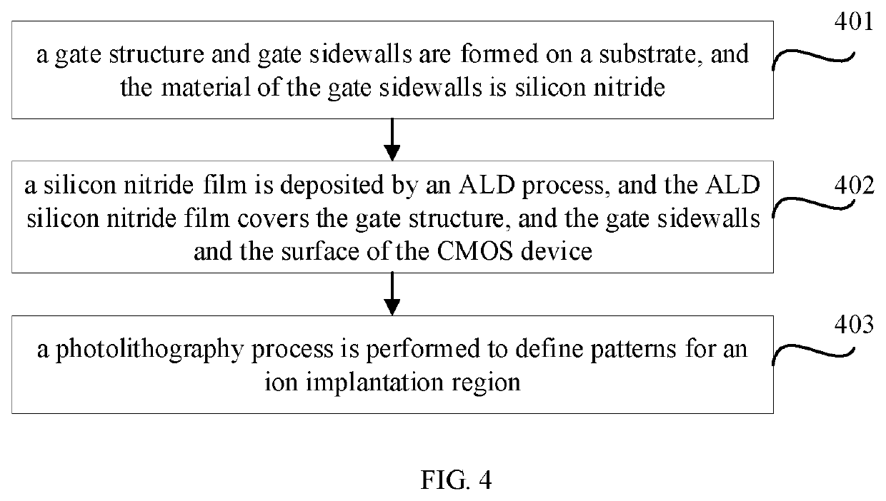
[0020]The technical solutions in this application will be clearly and completely described below with reference to the drawings. Obviously, the described embodiments are part of the embodiments of the application, instead of all them. Based on the embodiments in the present application, all other embodiments obtained by one skilled in the art without contributing any inventive labor shall fall into the protection scope of the present application.

[0021]In the description of this application, it should be noted that the orientation or positional relationship indicated by the terms “center”, “upper”, “lower”, “left”, “right”, “vertical”, “horizontal”, “inside”, “outside”, or the like is based on the orientation or positional relationship shown in the drawings, is only for the convenience of describing this application and simplified description, and does not indicate or imply that the indicated device or element must have a specific orientation or be configured and operated in a specif...


PUM

PropertyMeasurementUnit
temperatureaaaaaaaaaa
thicknessaaaaaaaaaa
structureaaaaaaaaaa

Abstract

A method for manufacturing a CMOS device includes: forming a gate structure and gate sidewalls of the CMOS device, wherein the material of the gate sidewalls is silicon nitride; depositing a silicon nitride film directly on the gate structure and the gate sidewalls, wherein the depositing is performed via atomic layer deposition (ALD); and performing a photolithography process to define an ion implantation region.

Description

CROSS-REFERENCES TO RELATED APPLICATIONS[0001]This application claims the priority to Chinese patent application No. CN201911107530.5 filed at CNIPA on Nov. 13, 2019, and entitled “METHOD FOR MANUFACTURING A CMOS DEVICE”, the disclosure of which is incorporated herein by reference in entirety.TECHNICAL FIELD[0002]The present disclosure relates to the field of semiconductor manufacturing, in particular to a method for manufacturing a CMOS device.BACKGROUND[0003]In mainstream integrated circuit (IC) manufacturing process, the sidewalls of a gate usually contains silicon nitride. However, photoresists applied in dozens of photolithography processes in making ICs are sensitive to nitrogen-containing materials. Thus, silicon nitride materials easily cause photoresist denaturation which generates an undesirable footing phenomenon. In order to solve the footing phenomenon, an oxygen plasma is often applied for interface treatment before any photolithography process currently.[0004]However,...

Claims


Application Information

Patent Timeline
Patent Type & Authority Patents(United States)
IPC IPC(8): H01L21/8238H01L21/02H01L21/265
CPCH01L21/823814H01L21/0217H01L21/0228H01L21/26513H01L21/823864H01L21/823878H01L21/8238H01L21/823828H01L27/092H01L21/266H01L21/2652H01L29/78H01L29/6656
Inventor LI, RUNLINGCHEN, XUEFEI
Owner SHANGHAI HUALI INTEGRATED CIRCUIT CORP
Why Eureka
Try Eureka