Subtractive - Additive Edge Defined Lithography

a technology of additive edge and lithography, which is applied in the direction of optics, instruments, photomechanical equipment, etc., can solve the problems of uneven topography and other problems, and achieve the effects of good adhesion, small grain size, and high selectivity

Inactive Publication Date: 2007-06-14
DUNNROWICZ CLARENCE JOHN
View PDF44 Cites 1 Cited by
  • Summary
  • Abstract
  • Description
  • Claims
  • Application Information

AI Technical Summary

Benefits of technology

[0018] Within scope of this invention it has been determined that a 10% titanium-tungsten (TiW) sputtered layer of approximately 20-30 nm uniquely meets above (VTF) requirements. This material is commonly utilized as a metal contact and diffusion barrier. It displays good adherence due to the titanium content, has small grain size, and most notably can be etched (subtracted) using essentially oxizidized water or hydrogen peroxide at room temperature. In addition, the (Ti, W) metal oxides display very high selectivity in oxygen plasmas, permitting precise patterning of underlying organic layers typically used in tri-level patterning schemes. Although not fully transparent, a TiW layer of this thickness is semi-transparent or partially absorbing, helping to reduce substrate reflections.
[0019] The combination of TiW as (VTF) and excellent selectivity of chemical etching allows the subtractive-additive bias to be very small. In essence, the (VTF) bias undercut in a stagnant etch solution is diffusion limited and highly uniform. Although the chemically etched TiW sidewall has in principle an isotropic profile, it has minor impact for a (VTF) which has high etch selectivity in subsequent process steps.
[0021] In one embodiment of this invention, this robust feature can be very usefull in decreasing the operational bias of a device while maintaining a high process yield as illustrated in FIG. 3. As illustrated, aluminum 10, 11 metal replaces the TiW / Ti 1 masking layers shown in FIGS. 1, 2, and polyimide layer 4 is omitted for fabricating a Surface Acoustic Wave (SAW) transducer. Similarly, FIG. 4 illustrates SAEDL technique applied to electrical interconnection of fine grating lines formed by interference lithography (IL) without the need for e-beam or focused ion beams.

Problems solved by technology

ARC are generally employed to control substrate reflections, but uneven topography remains a challenge.

Method used


Image

  • Subtractive - Additive Edge Defined Lithography
  • Subtractive - Additive Edge Defined Lithography
  • Subtractive - Additive Edge Defined Lithography

Examples


Embodiment Construction

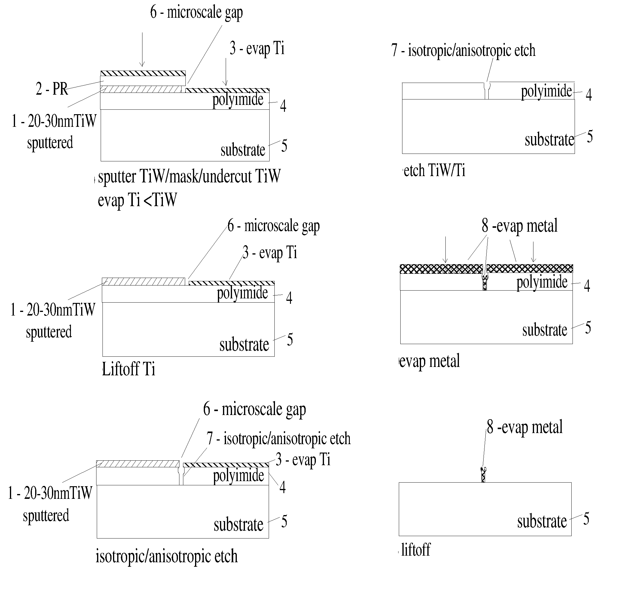
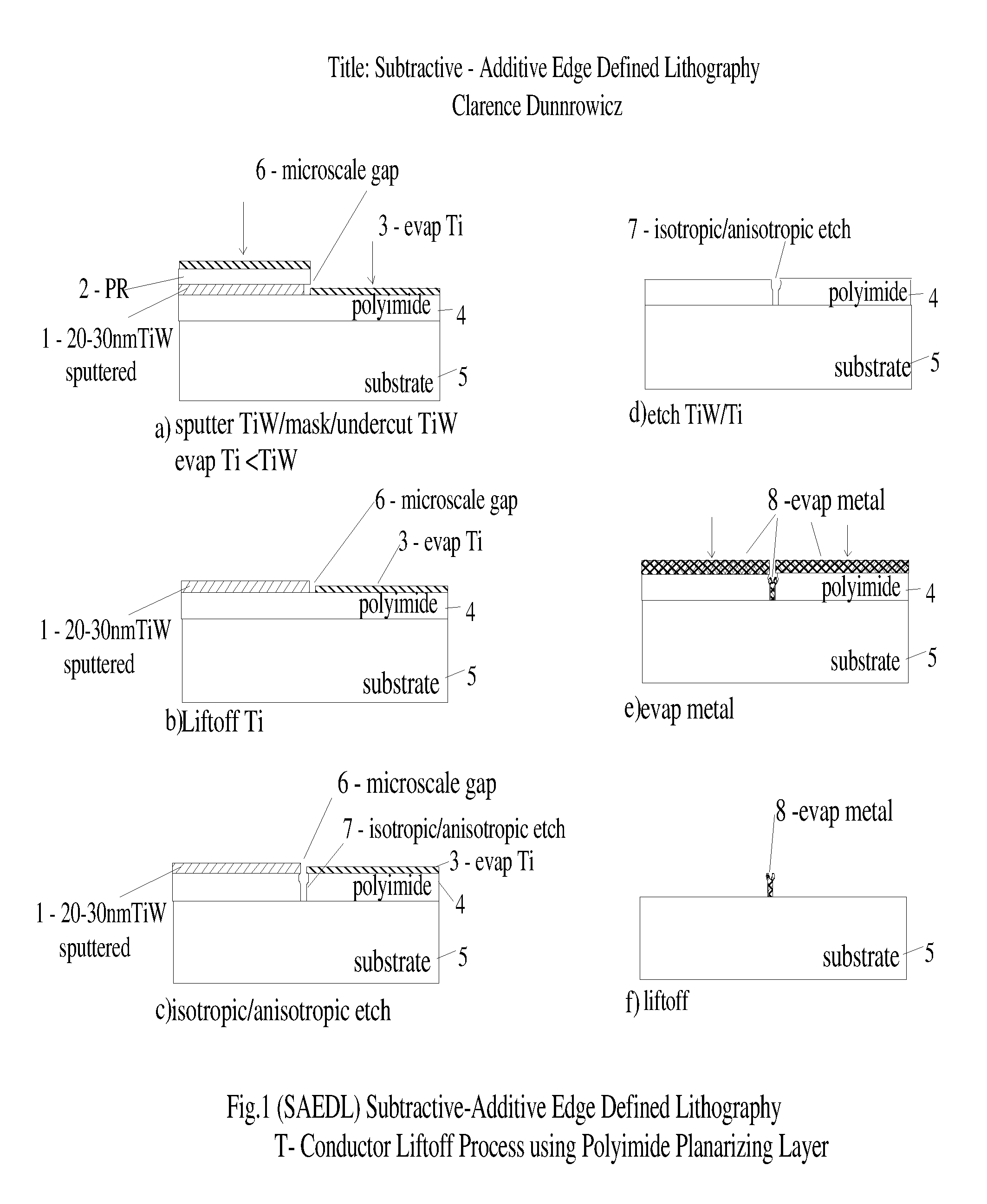
[0027]FIG. 1 is a section view illustrating the basic subtractive-additive edge defined lithographic (SAEDL) processing sequence with (TiW / Ti) masking films to generate a liftoff T-shaped metal conductor using a polyimide planarizing layer.

[0028] Follow polyimide 4 layer manufacturer recommended procedure for substrate 5 preparation. This typically involves hydrocarbon contamination removal and a desorption bake prior to application of an adhesion primer. Try to choose a polyimide 4 that approximately matches substrate 5 thermal expansion, but it is not critical as it is typically kept thin and not fully cured for this application. Viscosity and spin speed will depend on desired final dimensions of T-shaped conductor 8, etc. Dupont Pyralin series or similar have given good results. After spin, a prebake of approximately 100 deg. C. for 60 min., followed by 200 deg. C. for 60 min. in nitrogen has been found to give satisfactory stabilization.

[0029] Immediately load substrates 5 int...


PUM


Abstract

A subtractive-additive, differential lithography technique capable of generating sub-half micron geometries using a larger feature parent mask is described. The basic technique is defect tolerant with respect to electrical shorting, can fabricate T-shaped conductors of optimum geometry to minimize electrical RC time constant, and can be extended to very small, dense geometries by utilizing interference lithography or nano-imprint parent masks. Demonstration fabrication examples include a Surface Acoustic Wave (SAW) transducer, Field Effect Transistor (FET), and grating interconnection method.

Description

[0001] Conceptually, structure fabrication can be simplified into the basic elements of addition, subtraction, and reshaping. Noteworthy examples include the Golden Gate bridge, Michelangelo's David, and the ubiquitous nano-imprint molding of CD / DVD disks, respectively. [0002] Modern society is largely based upon the creative and highly refined application of these fundamental processes to the miniaturization and planarization of the basic transistor or switch. Pursuit of this goal by the direct fabrication of these microscale elements has resulted in rapid progress and an empirical scaling model commonly referred to as Moore's Law. It is the scope of this invention to demonstrate that micro-scale elements can also be realized by appropriately combining the indirect, differential technique of sequential subtractive and additive processes on larger scale elements. Inventor / Assignee: Clarence Dunnrowicz REFERENCES [0003] Henry I. Smith, “Fabrication Techniques for Surface Acoustic Wa...

Claims


Application Information

Patent Timeline
Patent Type & Authority Applications(United States)
IPC IPC(8): H01L21/425
CPCH01L21/0331H01L21/28114
Inventor DUNNROWICZ, CLARENCE JOHN
Owner DUNNROWICZ CLARENCE JOHN
Why Eureka
Try Eureka