Thin film fabrication method and thin film fabrication apparatus
Inactive Publication Date: 2001-07-26
ANELVA CORP
View PDF20 Cites 11 Cited by
Summary
Abstract
Description
Claims
Application Information
AI Technical Summary
This helps you quickly interpret patents by identifying the three key elements:
Problems solved by technology
Method used
Benefits of technology
Problems solved by technology
Arrival of a lot of sputter particles results in the growth of a thin film.
Consequently, these sputter particles cause considerable build-up at the hole opening edge portion, and a protuberance which is called overhang is liable to be formed.
When the aspect ratio becomes high, the amount of the sputter particles which can penetrate into the hole falls, with the consequence that the hole bottom surface coverage deteriorates.
However, with conventional methods and apparatus, problems may arise.
However, the ions also strike locations other than the overhang portion with high energy, and so cause resputtering of the thin film which is in the process of being built up or deposited.
Consequently, the overall film deposition rate becomes slower and productivity falls.
There is also the problem that, as the result of the process gas ions being incident at high energy, process gas ions become admixed in the thin film, so causing a lowering of the quality of the thin film that is produced.
Also, when the ion incidence quantity becomes large there is excessive accumulation of charge, and hence a problem of electrical damage to a device.
Method used
Image
Click on the blue label to locate the original text in one second.
Reading with bidirectional positioning of images and text.
Examples
first embodiment
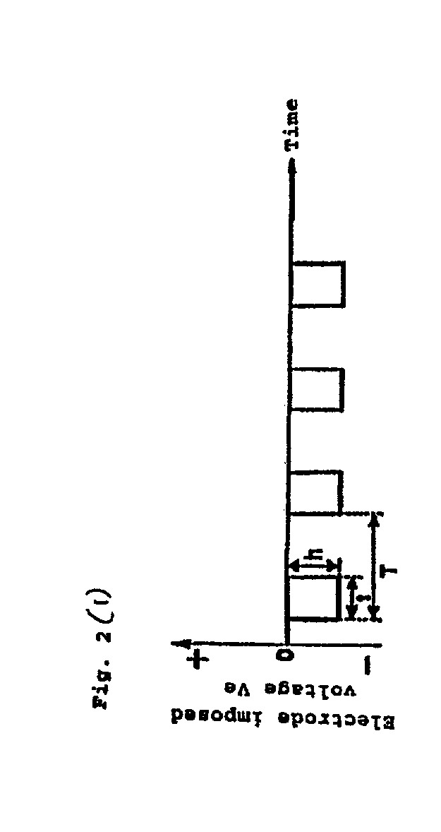
[0122] First, as an example of implementation associated with the first embodiment, the structure can be made such that an electrode imposed voltage Ve such as follows is imposed.
[0127] By way of an example of implementation of the second embodiment, the structure can be made such that an electrode imposed voltage Ve such as follows is imposed.
[0134] By way of an example of implementation of the third embodiment, the structure can be made such that an electrode imposed voltage Ve such as follows is imposed.
[0145] When film deposition is effected in conditions such as these, excellent results for practical purposes are achieved, the bottom coverage ratio (the ratio of the rate of hole bottom surface film deposition to that on surfaces other than the hole) for holes with a...
PUM
Property
Measurement
Unit
Time
aaaaa
aaaaa
Polarity
aaaaa
aaaaa
Electric potential / voltage
aaaaa
aaaaa
Abstract
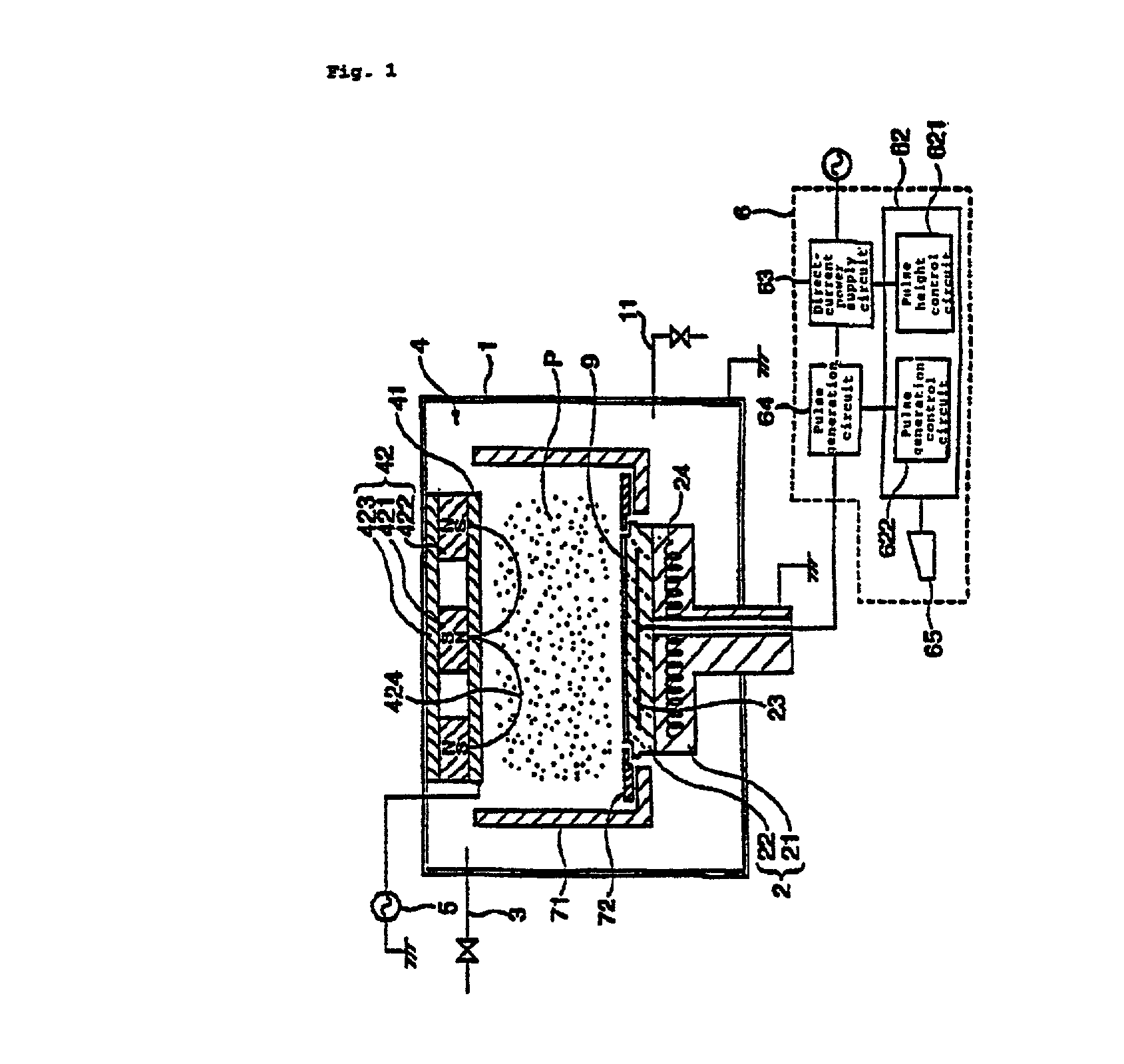
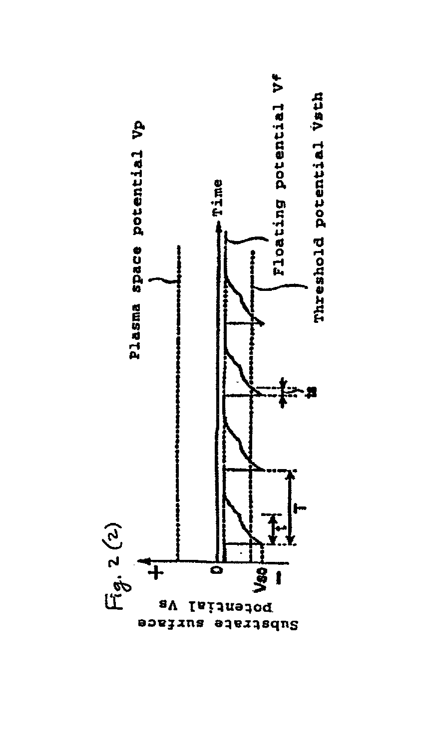
A thin film is fabricated while causing ions in a plasma P to be incident by effecting biasing relative to the space potential of the plasma P by imparting a set potential to the surface of a substrate 9. A bias system 6 causes the substrate surface potential Vs to vary in pulse form by imposing an electrode imposed voltage Ve in pulse form on a bias electrode 23 which is in a dielectric block 22. The pulse frequency is lower than the oscillation frequency of ions in the plasma P, and the pulse period T, pulse width t and pulse height h are controlled by a control section 62 in a manner such that the incidence of ions is optimized. The imposed pulses are controlled in a manner such that the substrate surface potential Vs recovers to a floating potential Vf at the end of a pulse period T, and that the ion incidence energy temporarily crosses a thin film sputtering threshold value in a pulse period T.
Description
[0001] Referenced-Applications[0002] This application claims the priority of Japanese Patent Application No. 11-066067, filed on Mar. 12, 1999 in Japan, the entire contents of which are hereby incorporated herein by reference.[0003] Not ApplicableREFERENCE TO A MICROFICHE APPENDIX[0004] Not ApplicableBACKGROUND OF THE INVENTION DESCRIPTION OF RELATED ART[0005] Thin film fabrication processes such as sputtering and CVD are widely employed in the manufacture of LSI and various other electronic devices and display devices such as liquid crystal displays, etc. Meanwhile, greater and greater advances are being made in device integration and miniaturization in the field of semiconductor devices. Device miniaturization demands new techniques in device manufacture. More specifically, aspects involved comprise the filling of very fine holes with sufficient amounts of film, measures to reduce step differences in device manufacture, and the prevention of lead breakage due to electron migration...
Claims
Application Information
Patent Timeline
Application Date:The date an application was filed.
Publication Date:The date a patent or application was officially published.
First Publication Date:The earliest publication date of a patent with the same application number.
Issue Date:Publication date of the patent grant document.
PCT Entry Date:The Entry date of PCT National Phase.
Estimated Expiry Date:The statutory expiry date of a patent right according to the Patent Law, and it is the longest term of protection that the patent right can achieve without the termination of the patent right due to other reasons(Term extension factor has been taken into account ).
Invalid Date:Actual expiry date is based on effective date or publication date of legal transaction data of invalid patent.

