Semiconductor device and manufacturing method thereof

a technology of semiconductors and semiconductors, applied in the direction of identification means, instruments, optics, etc., can solve the problems of reduced aperture ratio, easy generation of signal delay, and display becoming darker

Inactive Publication Date: 2001-10-04
SEMICON ENERGY LAB CO LTD
View PDF0 Cites 126 Cited by
  • Summary
  • Abstract
  • Description
  • Claims
  • Application Information

AI Technical Summary

Problems solved by technology

With a liquid crystal display panel in which a color filter is formed in the opposing substrate, it is necessary to perform assembly of the element substrate and the opposing substrate with extremely high precision, and when this precision is low, a the aperture ratio is reduced and there is a problem in which the display becomes darker.
Further, with a liquid crystal display panel in which a metallic film is used as a shading mask, a problem develops in which a signal delay easily generates due to a parasitic capacitance with other wirings.
Furthermore, when an organic film is used, a problem that the number of process steps increases is caused.
In addition, with an EL display device using an EL element for emitting light showing a red color, a green color, or a blue color, the EL material differs for each color, and therefore the element characteristics also differ, and it becomes difficult to obtain a uniform display.
For example, characteristics such as the deterioration speed of the EL material differ for each material, and therefore a problem in which the displays become dispersed due to elapsed time develops.
Furthermore, an EL display device using an EL element which emits white color light is, in principle, similar to a liquid crystal display device using a color filter, and therefore problems similar to those above develop.

Method used


Image

  • Semiconductor device and manufacturing method thereof
  • Semiconductor device and manufacturing method thereof
  • Semiconductor device and manufacturing method thereof

Examples


embodiment 1

[0090] [Embodiment 1]

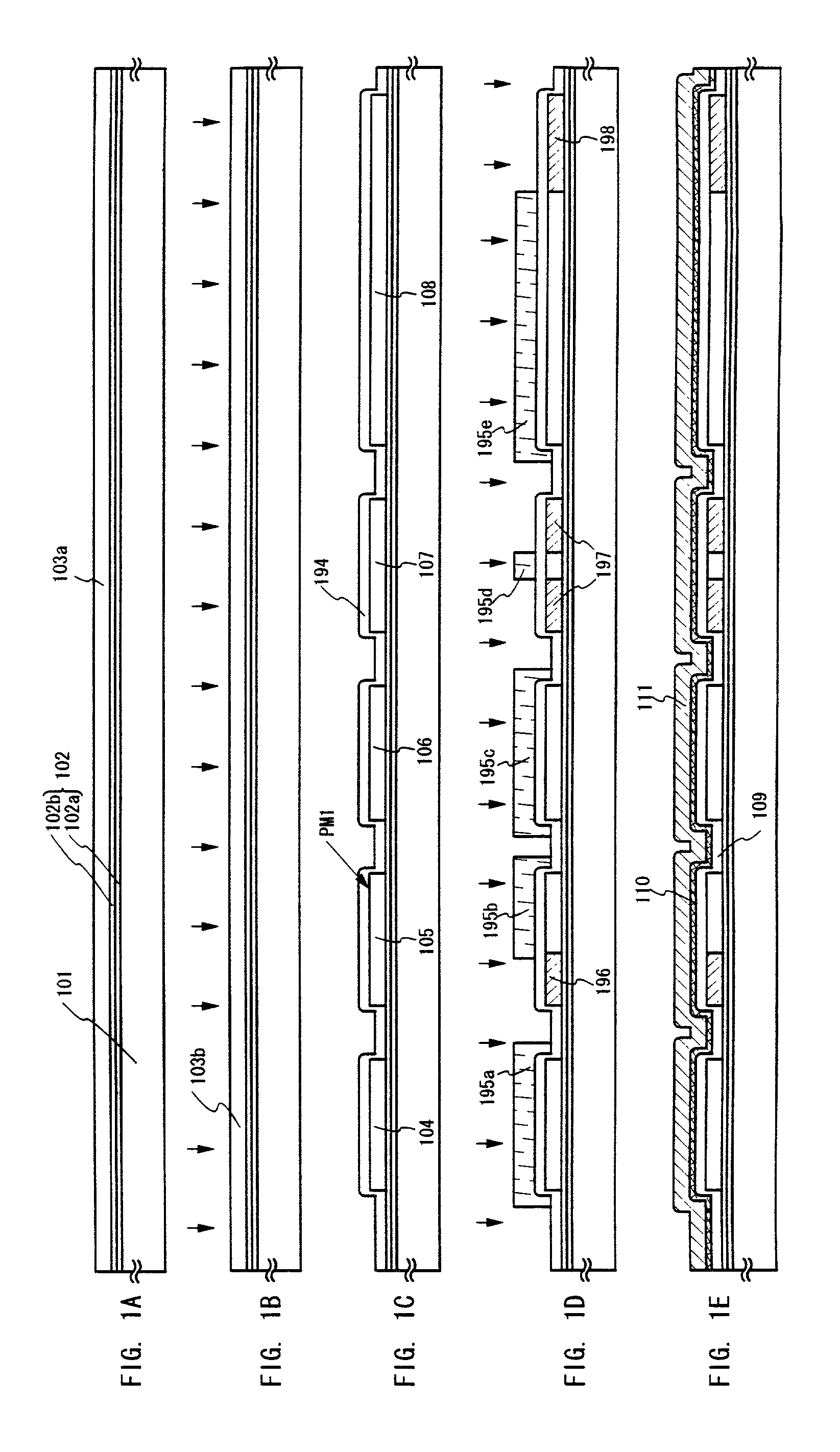
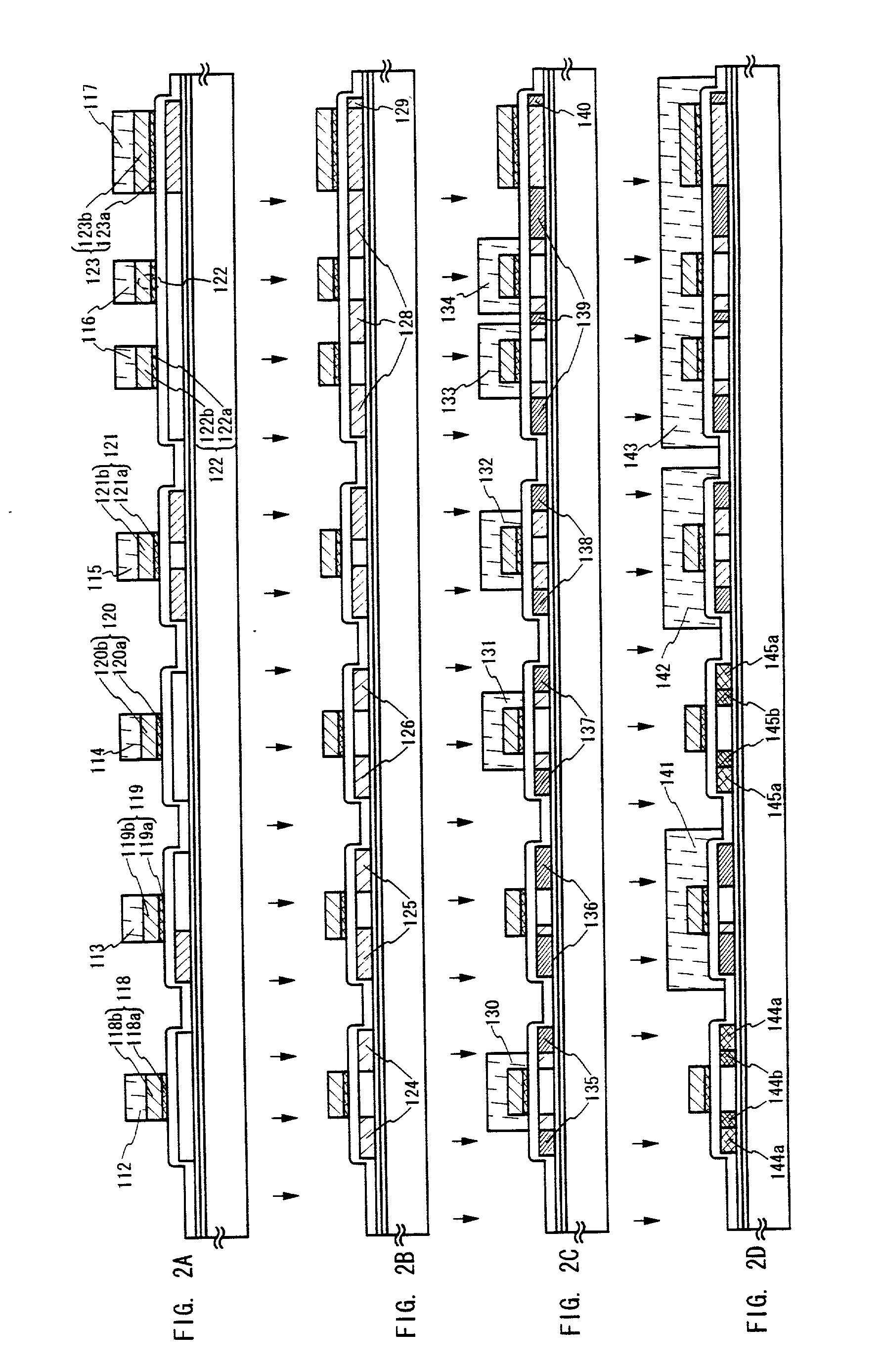
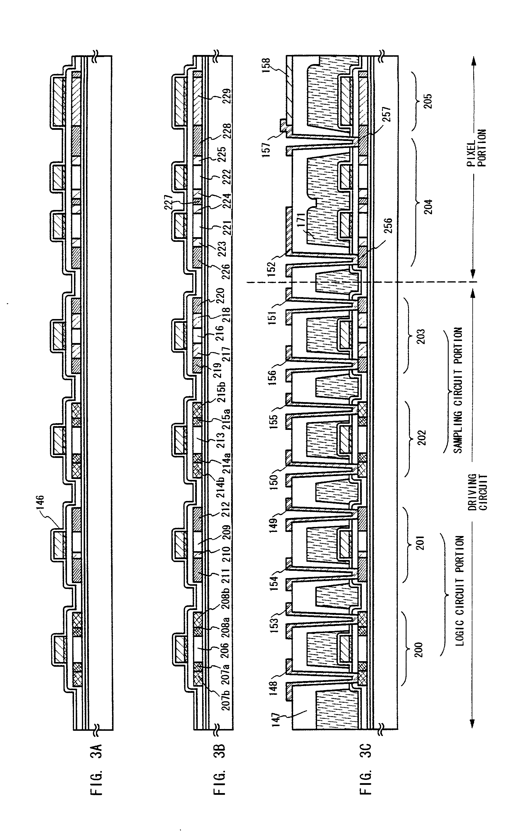
[0091] An embodiment of the present invention will be explained with reference to FIGS. 1A to 3C. In this embodiment, a method of forming simultaneously pixel TFTs and storage capacitors of a pixel section and TFTs of a driving circuit disposed in the periphery of the display region will be explained step-wise in detail.

[0092] In FIG. 1A, as well as barium borosilicate glass or aluminoborosilicate glass as typified by Corning #7059 glass and #1737 glass, plastic substrates which do not have optical anisotropy such as polyethylene terephthalate (PET), polyethylene naphthalate (PEN), polyethersulfone (PES), etc., can be used as the substrate 101. When the glass substrate is used, the substrate may be heat-treated in advance at a temperature lower by about 10 to 20.degree. C. than a glass strain point. A base film 102 of a silicon oxide film, a silicon nitride film or a silicon oxynitride film, etc. is formed on the surface of the substrate 101, on which TFT is to ...

embodiment 2

[0124] [Embodiment 2]

[0125] In this embodiment, the forming method of a pixel electrode is shown, which is different from that of Embodiment 1. Same marks as Embodiment 1 are used, because all structure are same as Embodiment 1 other than overlapping portion of the pixel electrode in pixel portion and the drain wiring.

[0126] FIG. 5A shows a cross sectional structure in the pixel portion. In this embodiment, after forming the contact hole on the interlayer insulating film, the drain wiring 357 is formed which is composed of a compound layer; Ti film 357a, Al film 357b and Ti film 357c. And the pixel electrode 358 is formed to be composed a portion of the wiring.

embodiment 3

[0127] [Embodiment 3]

[0128] To accomplish a high-precision and high-quality liquid crystal display device, the characteristics of the TFT constituting the each circuit of the pixel TFT and the driving circuit must be improved. One of the required TFT characteristics is the decrease of the current flowing under the OFF state (OFF current) besides the threshold voltage, the field effect mobility, the sub-threshold coefficient (S value), and so forth. When the OFF current value is high, not only the power consumption increases, but also the operation characteristics of the driving circuit get deteriorated and may invite the drop of image quality. In the n-channel TFT fabricated in Embodiment 1, the LDD region is formed, and this LDD region can lower the OFF current value to the extent that renders no problem. On the other hand, since the p-channel TFT has the single drain structure, the increase of the OFF current value often becomes the problem. This embodiment provides a method of fa...


PUM

PropertyMeasurementUnit
angleaaaaaaaaaa
thickaaaaaaaaaa
glass strain pointaaaaaaaaaa

Abstract

There is a problem in that, in a liquid crystal display panel in which a color filter is formed on an opposing substrate, it is necessary to assemble an element substrate and the opposing substrate by extremely high precision position alignment, and when this precision is low, the aperture ratio decreases and the display becomes darker. With the present invention, red color filters (R) are formed on driving circuits (402, 403), peripheral circuits, and a color filter (405d) for protecting a pixel TFT portion (407) is formed for each pixel.

Description

[0001] 1. Field of the Invention[0002] The present invention relates to a semiconductor device containing a circuit structured by a thin film transistor (hereafter referred to as a TFT), and to a method of manufacturing thereof. For example, the present invention relates to an electro-optical device, typically a liquid crystal display panel or an EL display panel, and to electronic equipment (electronic instruments) loaded with this type of electro-optical device (electronic device) as a part.[0003] Note that, throughout this specification, the term semiconductor device indicates general devices which function by utilizing semiconductor characteristics, and that electro-optical devices, semiconductor circuits, and electronic equipment are all semiconductor devices.[0004] 2. Description of the Related Art[0005] Techniques of structuring a thin film transistor (TFT) using a semiconductor thin film (having a thickness on the order of several nm to several hundreds of nm) formed on a su...

Claims


Application Information

Patent Timeline
Patent Type & Authority Applications(United States)
IPC IPC(8): G02F1/1335G02F1/136G02F1/1362G02F1/1368H01L21/336H01L21/768G09F9/30H01L21/77H01L21/84H01L23/522H01L27/12H01L27/32H01L29/786
CPCG02F1/133514G02F1/13454G02F1/136227H01L27/12H01L27/3244H01L27/1248H01L29/4908H01L29/66757H01L29/78621H01L2029/7863H01L27/124H01L29/458H10K59/38H10K59/12
Inventor YAMAZAKI, SHUNPEIKUWABARA, HIDEAKI
Owner SEMICON ENERGY LAB CO LTD
Why Eureka
Try Eureka