

Electrostatic chucking device and manufacturing method thereof
a technology of chucking device and chucking sheet, which is applied in the direction of chucking device, mechanical equipment, transportation and packaging, etc., can solve the problems that the chucking sheet is gradually peeled off from the outer peripheral portion of the chucking sheet and the heat resistance is excellent. excellent, the effect of excellent heat resistan
- Summary
- Abstract
- Description
- Claims
- Application Information
AI Technical Summary
Benefits of technology
Problems solved by technology
Method used
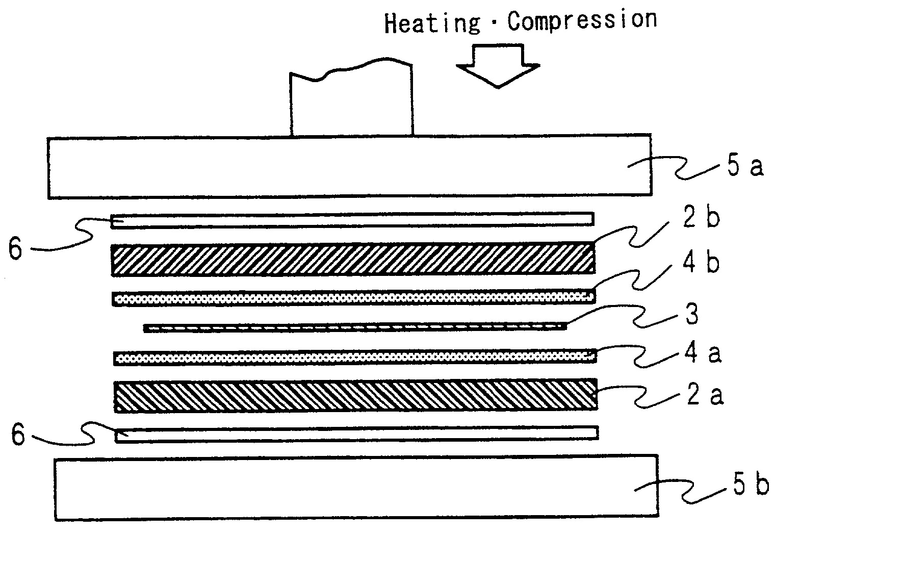
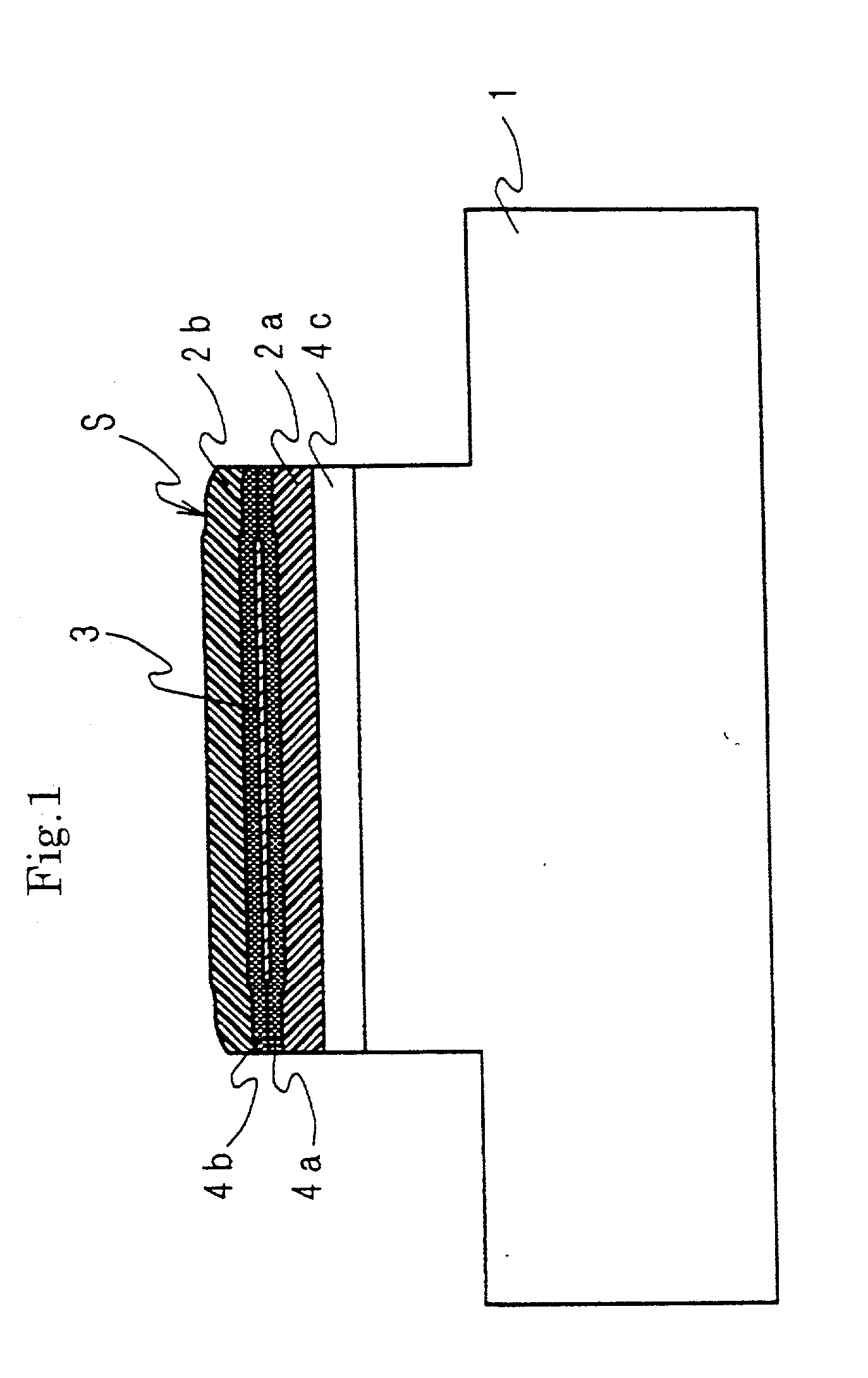
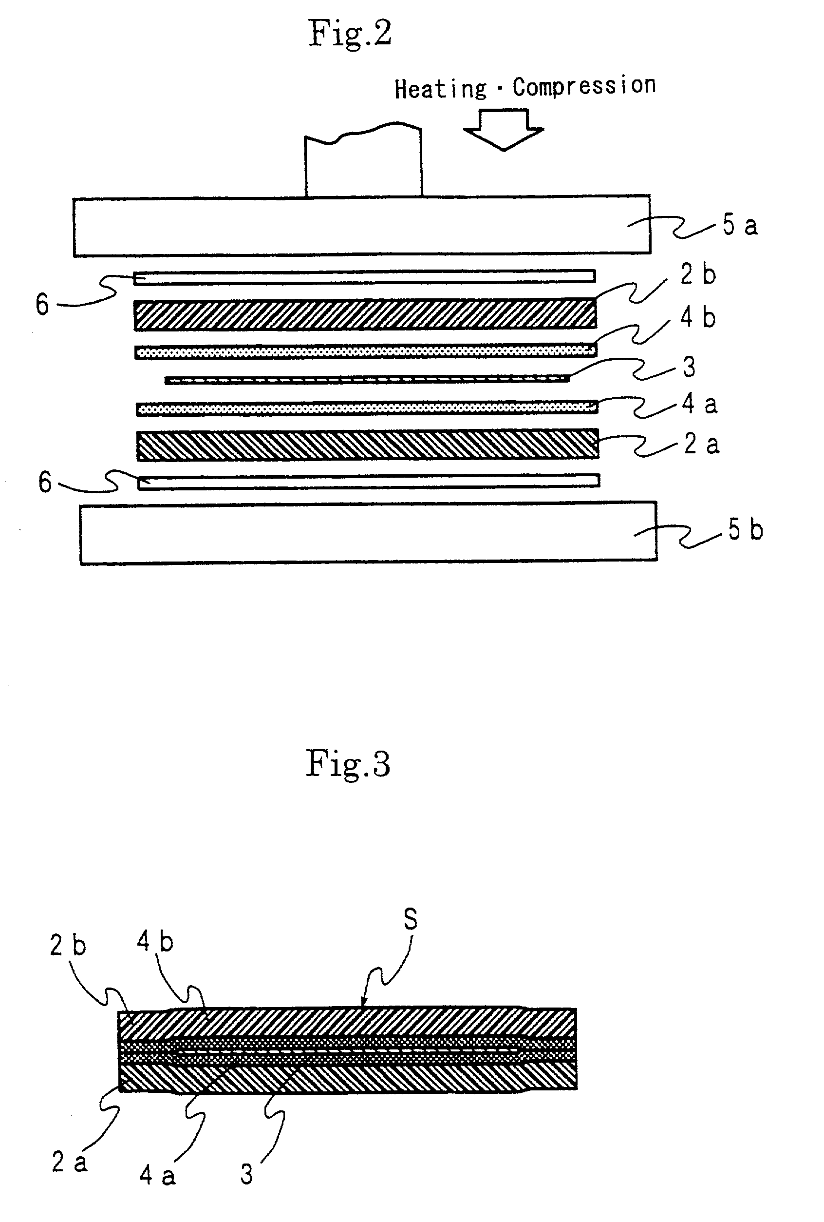
Image

Examples
experimental example 1
[0041] With respect to the electrostatic chucking device obtained by the embodiment 1, an attraction force was measured using an electrostatic chucking attraction force measuring device (made by Creative Technology Ltd.) shown in FIG. 5 and the evaluation on the attraction force was conducted.
[0042] First of all, as shown in FIG. 5, in the inside of a vacuum chamber 10 of the measuring device, the electrostatic chucking device is set such that a He gas supply port 11 of the vacuum chamber 10 is communicably connected with a through hole 7 which penetrates the electrostatic chucking device from a lower surface to an upper surface of the electrostatic chucking device. A silicon wafer W is set on the electrostatic chucking sheet S of this electrostatic chucking device. Until the pressure in the inside of the vacuum chamber 10 is reduced to 0.1 Pa, gas is exhausted from an exhaust port 12. In this state, a DC voltage of 1.5 kV is applied to an electrode layer 3 of the electrostatic chuc...
experimental example 2
[0044] While maintaining the gas pressure of the He gas in the inside of the vacuum chamber 10 at 1000 Pa, the temperature distribution within a surface of the silicon wafer was measured by using a temperature measurement wafer (name of product produced by Creative Technology Ltd: Tc wafer) which mounts thermocouples at the center of a 8 inch wafer, at 3 to 9 positions on a circumference having a diameter of 90 mm of the wafer and at 3 to 9 positions on a circumference having a diameter of 180 mm of the wafer so as to measure the temperature distribution at respective positions. The result shows that the temperature distribution within the surface of the silicon wafer was .+-.1.0.degree. C.
experimental example 3
[0045] Further, the electrostatic chucking device obtained by the embodiment 1 was mounted on an actual parallel flat-plate type plasma etching device and an etching test was performed.
[0046] In this parallel flat-plate type plasma etching device, the electrostatic chucking device is installed in the inside of a reaction chamber and an upper shower electrode is disposed right above the electrostatic chucking device. An output of a high frequency power supply having a frequency of 13.56 MHz and an output of 1500 W is connected to the aluminum substrate of the electrostatic chucking device. Further, the upper shower electrode is grounded and a reactive gas pipe is connected to a rear surface of the upper shower electrode to supply reactive gas through shower holes. Further, an output of a DC power supply having a voltage of 1.5 kV is connected to an attraction electrode of the electrostatic chucking device.
[0047] On the attraction surface of the electrostatic chucking device installed...
PUM
| Property | Measurement | Unit |
|---|---|---|
| thickness | aaaaa | aaaaa |
| thickness | aaaaa | aaaaa |
| temperature | aaaaa | aaaaa |
Abstract
Description
Claims
Application Information