Low k dielectric materials with inherent copper ion migration barrier

a technology of low k dielectric materials and migration barriers, which is applied in the direction of electrical apparatus, semiconductor devices, semiconductor/solid-state device details, etc., can solve the problems of reducing the overall dielectric constant reducing the performance of the chip, and increasing the overall dielectric constant performan

Inactive Publication Date: 2002-03-21
IBM CORP
View PDF0 Cites 1 Cited by
  • Summary
  • Abstract
  • Description
  • Claims
  • Application Information

AI Technical Summary

Problems solved by technology

The utilization of such high dielectric constant Cu ion migration barriers is not practical with today's generation of IC chips; the employment of the same increases the overall dielectric constant of the IC chip, i.e. the sum of the dielectric constant of the ion migration barrier layer plus that of the interlayer dielectric (ILD) times their respective thickness.
The higher the dielectric constant of the ILD, the lower the performance of the chip.
The manufacture of separate dielectric barrier layers not only increases the overall dielectric constant deteriorating chip performance, but also adds additional processing steps which add to the complexity and cost of chip manufacturing.
To date, no successful use of only a low k ILD as a Cu ion migration barrier has been realized since such materials readily permit Cu ion migration.

Method used


Image

  • Low k dielectric materials with inherent copper ion migration barrier
  • Low k dielectric materials with inherent copper ion migration barrier
  • Low k dielectric materials with inherent copper ion migration barrier

Examples


Embodiment Construction

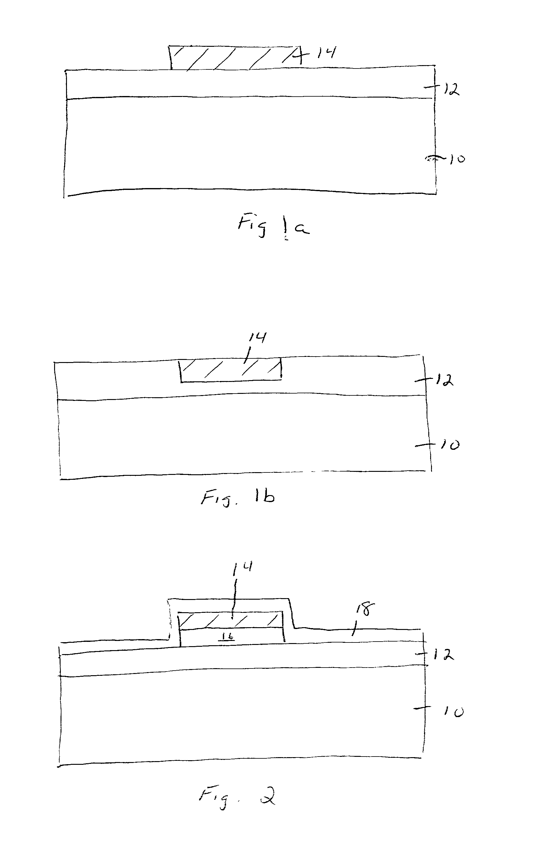
[0036] In this example, the following studies were performed on structures which contained the interlayer dielectric of the present invention, i.e. thermosetting polyarylene ether containing a phthalocyanine derivative, i.e. 2,9, 16, 23-tetra-tert-butyl-29 H, 31 H phthalocyanine, as an additive, and comparison was made to structures that contained a conventional unmodified interlayer low k dielectric (thermosetting polyarylene ether without an additive).

[0037] Bias Thermal Stress (BTS) Test

[0038] BTS tests were used as an accelerated reliability test method for degradation of the above-mentioned interlayer dielectrics.

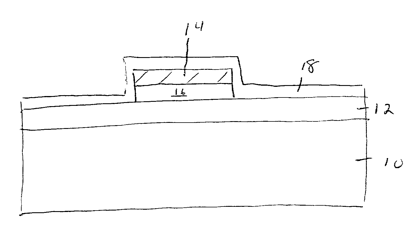
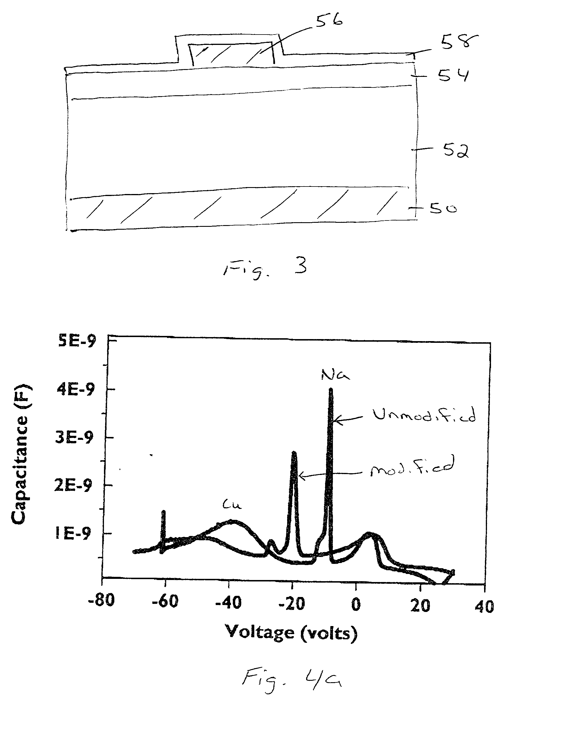
[0039] To measure the metallic ion migration through the above-mentioned dielectric materials, a capacitor structure such as shown in FIG. 3 was employed. Specifically, the structure shown in FIG. 3 comprises a bottom W electrode 50, a Si substrate 52, an interlayer dielectric 54, Cu or Al electrode 56, and Si.sub.3N.sub.4 layer 58.

[0040] In the test, a voltage of abou...


PUM

PropertyMeasurementUnit
dielectric constantaaaaaaaaaa
thicknessaaaaaaaaaa
thicknessaaaaaaaaaa

Abstract

An interlayer dielectric for preventing Cu ion migration in semiconductor structure containing a Cu region is provided. The interlayer dielectric of the present invention comprises a dielectric material that has a dielectric constant of 3.0 or less and an additive which is highly-capable of binding Cu ions, yet is soluble in the dielectric material. The presence of the additive in the low k dielectric allows for the elimination of conventional inorganic barrier materials such as SiO2 or Si3N4.

Description

[0001] The present invention relates to integrated circuits (ICs), and in particular to an interlayer dielectric which is capable of reducing or eliminating copper (Cu) ion migration in ICs. The interlayer dielectric of the present invention comprises a low dielectric constant dielectric material (k of 3.0 or less) that is modified to include an additive that has a high affinity for Cu ions, yet is soluble in the dielectric matrix.PRIOR ART[0002] In current IC chip designs which utilize copper (Cu) lines and organic, low k dielectrics as an interlayer dielectric, Cu ion migration barriers are typically made of high dielectric constant (k greater than 3.0) inorganic dielectrics such as silicon nitride or silicon dioxide. These inorganic dielectrics which are typically positioned between the interlayer dielectric and the Cu lines are used to reduce or eliminate Cu ion migration under electrical bias. Cu ion migration under electrical bias can occur under typical working conditions of ...

Claims


Application Information

Patent Timeline
Patent Type & Authority Applications(United States)
IPC IPC(8): H01L21/28H01L21/312H01L21/314H01L23/532H01L21/20H01L29/51
CPCH01L21/28194H01L21/312H01L21/3121H01L21/3146H01L23/53228H01L23/5329H01L29/513H01L29/517H01L2924/12044H01L2924/0002H01L21/02118H01L21/02115H01L2924/00H01L21/20
Inventor COHEN, STEPHAN ALANFEGER, CLAUDIUSHEDRICK, JEFFREY CURTISSHAW, JANE MARGARET
Owner IBM CORP
Why Eureka
Try Eureka