Spiral inductor and method for fabricating semiconductor integrated circuit device having same

a spiral inductor and integrated circuit technology, applied in the manufacture of inductances, solid-state devices, inductance/transformers/magnets, etc., can solve the problems of lowering the deterioration of the characteristics (q-value) of the inductor

Inactive Publication Date: 2002-03-28
KK TOSHIBA
View PDF2 Cites 37 Cited by
  • Summary
  • Abstract
  • Description
  • Claims
  • Application Information

AI Technical Summary

Problems solved by technology

However, if a plane spiral inductor is actually formed on a substrate, there is a problem in that it is not possible to sufficiently suppress a coupling between the spiral wiring and the substrate, so that part of high-frequency energy escapes into the substrate, thereby lowering characteristics (Q-value) of the inductor.
However, if the dummy elements are provided, there are two new problems as follows.
This means that a layer having a very low resistance is formed directly below the inductor, so that there is a problem in that characteristics (Q-value) of the inductor deteriorate.

Method used


Image

  • Spiral inductor and method for fabricating semiconductor integrated circuit device having same
  • Spiral inductor and method for fabricating semiconductor integrated circuit device having same
  • Spiral inductor and method for fabricating semiconductor integrated circuit device having same

Examples


first embodiment

(1) First Embodiment

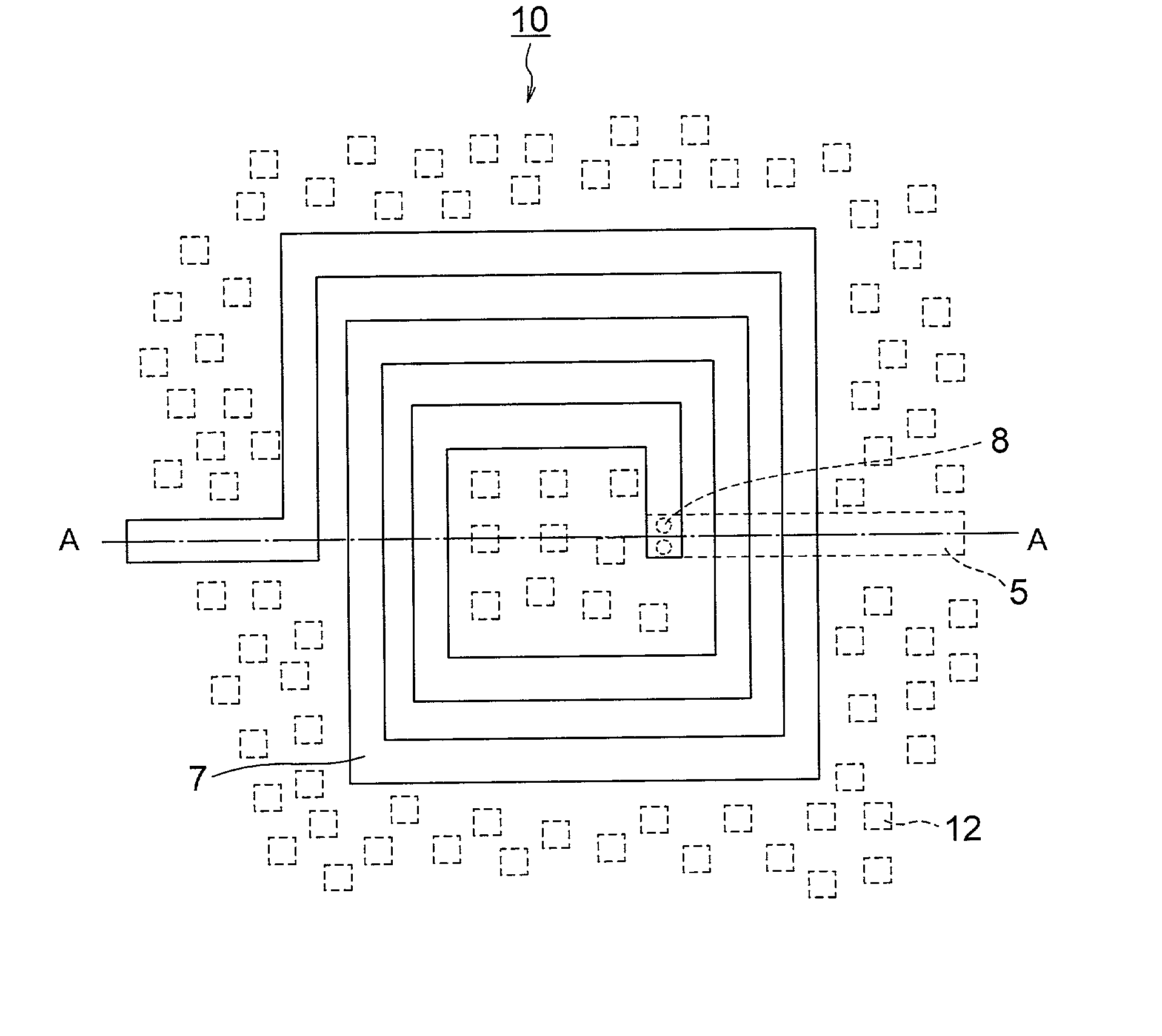
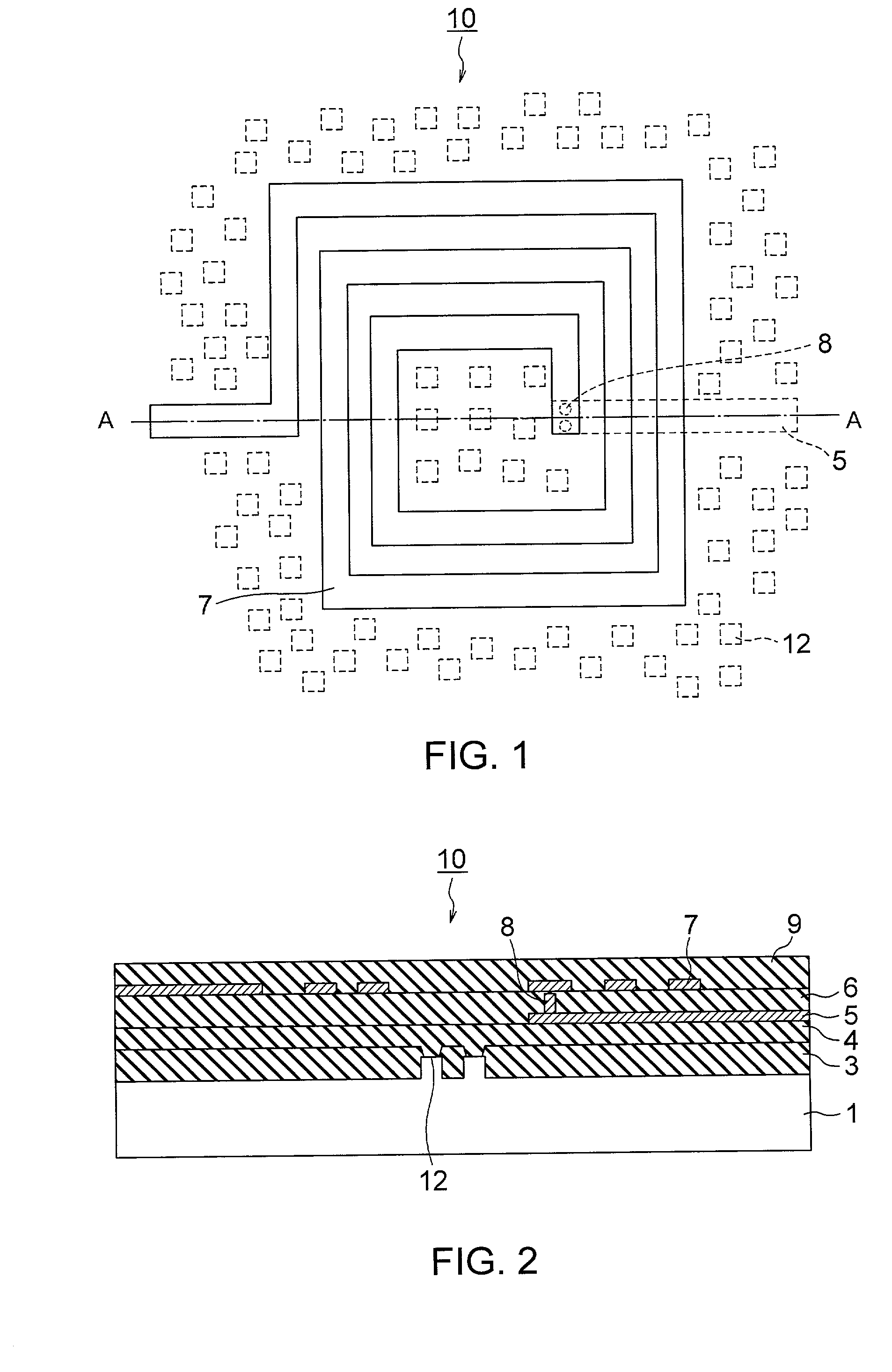
[0039] FIG. 1 is a plan view of the first embodiment of a spiral inductor according to the present invention, and FIG. 2 is a schematic sectional view taken along line A-A of FIG. 1.

[0040] As can be clearly seen from the comparison with FIGS. 19 and 20, the spiral inductor 10 shown in FIGS. 1 and 2 has a dummy element 12 which is arranged on the surface of the substrate 1 in regions other than those directly below spiral wiring portions 5 and 7. By forming the spiral inductor with such a structure, it is possible to decrease the coupling of the spiral wiring portions 5, 7 and the substrate 1 while suppressing dishing due to the CMP to the minimum. As a result, the leakage of high-frequency waves can be reduced, and the Q-value of the inductor can be maintained to be a large value.

[0041] The size of the spiral inductor 10 is hundreds .mu.m square. Other constructions of the spiral inductor 10 are substantially the same as those of the spiral inductor 100 shown in ...

second embodiment

(2) Second Embodiment

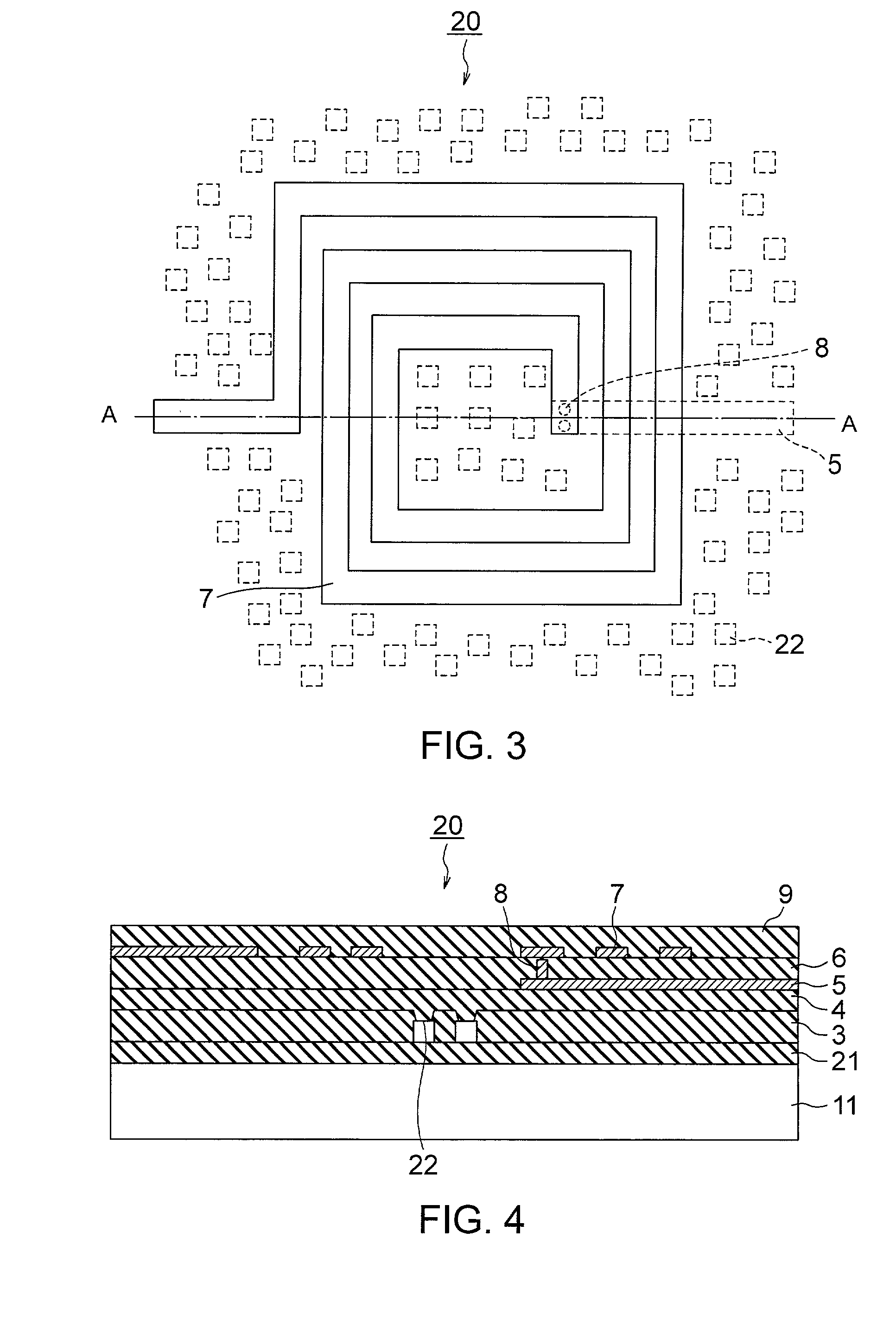
[0042] FIG. 3 is a plan view of the second embodiment of a spiral inductor according to the present invention, and FIG. 4 is a schematic sectional view taken along line A-A of FIG. 3. In this embodiment, the above described first embodiment is applied to an SOI (Silicon On Insulator) substrate.

[0043] A spiral inductor 20 in this embodiment comprises: a substrate 11; an insulating film 21 which is formed on the substrate 11; and a dummy element 22 which is formed by etching an SOI layer formed on the insulating film 21, in place of the substrate 1 and dummy element 12 of the spiral inductor 10 shown in FIGS. 1 and 2. The insulating film 21 is a buried oxide film for isolating the SOI layer from the supporting substrate 11. Other constructions of the spiral inductor 20 are substantially the same as those of the spiral inductor 10 shown in FIGS. 1 and 2. Similar to the dummy element 12 shown in FIGS. 1 and 2, the dummy element 22 is arranged in regions other than t...

third embodiment

(3) Third Embodiment

[0045] FIG. 5 is a plan view of the third embodiment of a spiral inductor according to the present invention, and FIG. 6 is a schematic sectional view taken along line A-A of FIG. 5.

[0046] The spiral inductor 30 shown in FIGS. 5 and 6 has a size of from about 100 .mu.m square to about 200 .mu.m square. As can be clearly seen from the comparison with FIGS. 1 and 2, the spiral inductor 30 has the lattice-shaped dummy element 32 with portions in regions corresponding to those directly below spiral wiring portions 5 and 7 being removed and the central and peripheral portions still remaining. Such a shape is particularly effective when the size of the inductor is relatively small as this embodiment. Other constructions of the spiral inductor 30 are substantially the same as those of the spiral inductor 10 shown in FIGS. 1 and 2.

[0047] Since the spiral inductor 30 in this embodiment thus has the lattice-shaped dummy element 32 from which portions in regions correspondi...


PUM

PropertyMeasurementUnit
conductiveaaaaaaaaaa
inductanceaaaaaaaaaa
frequencyaaaaaaaaaa

Abstract

A spiral inductor comprising: a substrate; a protruding portion which is formed on the top face of the substrate and the top of which serves as a dummy element for controlling a chemical mechanical polishing process; and a conductive layer which is formed on the substrate so as to have a spiral shape and which serves as an induction element, wherein the protruding portion is formed in a region other than a region directly below the conductive layer.

Description

[0001] This application claims benefit of priority under 35USC .sctn. 119 to Japanese patent application No. 2000-295823, filed on Sep. 28, 2000, the contents of which are incorporated by reference herein.[0002] 1. Field of the Invention[0003] The present invention relates generally to a spiral inductor serving as an inductance element spirally formed on a substrate, and a method for fabricating a semiconductor integrated circuit device having the same.[0004] 2. Related Background Art[0005] As one of inductance function elements provided in a semiconductor integrated circuit device (which will be simply hereinafter referred to as an IC), there is a so-called plane spiral inductor. This is designed to obtain a required inductance with such a structure that a plane spiral wiring is formed on a substrate.[0006] However, if a plane spiral inductor is actually formed on a substrate, there is a problem in that it is not possible to sufficiently suppress a coupling between the spiral wirin...

Claims


Application Information

Patent Timeline
Patent Type & Authority Applications(United States)
IPC IPC(8): H01L21/822H01F17/00H01F41/04H01L21/02H01L27/04H01L27/08
CPCH01F17/0006H01F41/042H01F2017/0046H01L27/08H01L28/10
Inventor MINAMI, YOSHIHIRO
Owner KK TOSHIBA
Why Eureka
Try Eureka