Cross-correlation timing calibration for wafer-level IC tester interconnect systems

a technology of interconnection system and cross-correlation timing, which is applied in the field of system for calibrating signal timing of ic wafer tester, can solve the problems of delay in signal path transmission, slightly different transmission times or rates, and adversely affecting channel ability

Inactive Publication Date: 2002-04-25
FORMFACTOR INC
View PDF0 Cites 37 Cited by
  • Summary
  • Abstract
  • Description
  • Claims
  • Application Information

AI Technical Summary

Problems solved by technology

Even when the TEST signal is as close as possible in phase to the REF signal, jitter and noise in the TEST and REF signals will cause them to transition at slightly different times or rates.
However the TEST signals that can be generated during a test can have a wide range frequencies, and the inherent delay of signal paths conveying the TEST signals to the IC under test can be frequency dependent.
In high frequency appli

Method used


Image

  • Cross-correlation timing calibration for wafer-level IC tester interconnect systems
  • Cross-correlation timing calibration for wafer-level IC tester interconnect systems
  • Cross-correlation timing calibration for wafer-level IC tester interconnect systems

Examples


Embodiment Construction

)

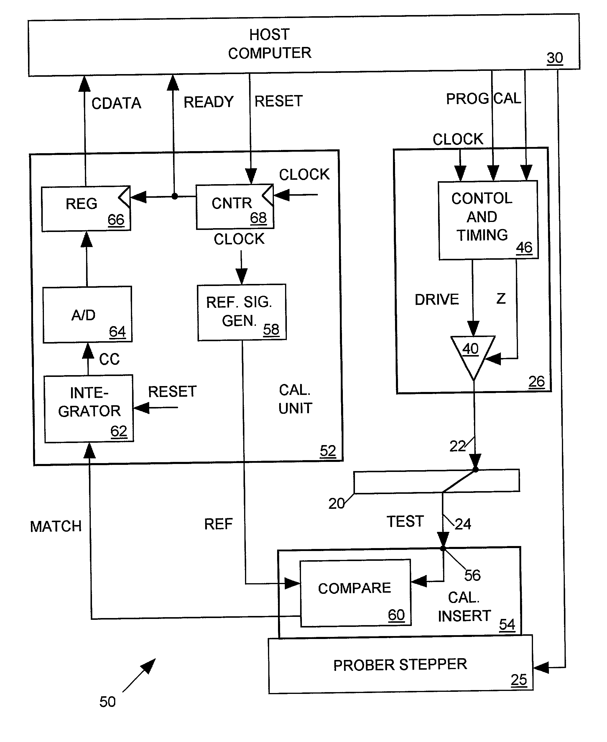
[0031] The present invention relates to a method and apparatus for accurately calibrating the event timing system of an integrated circuit (IC) tester. We will first describe the event timing system employed by a typical prior art IC tester and then describe how the present invention calibrates that timing system.

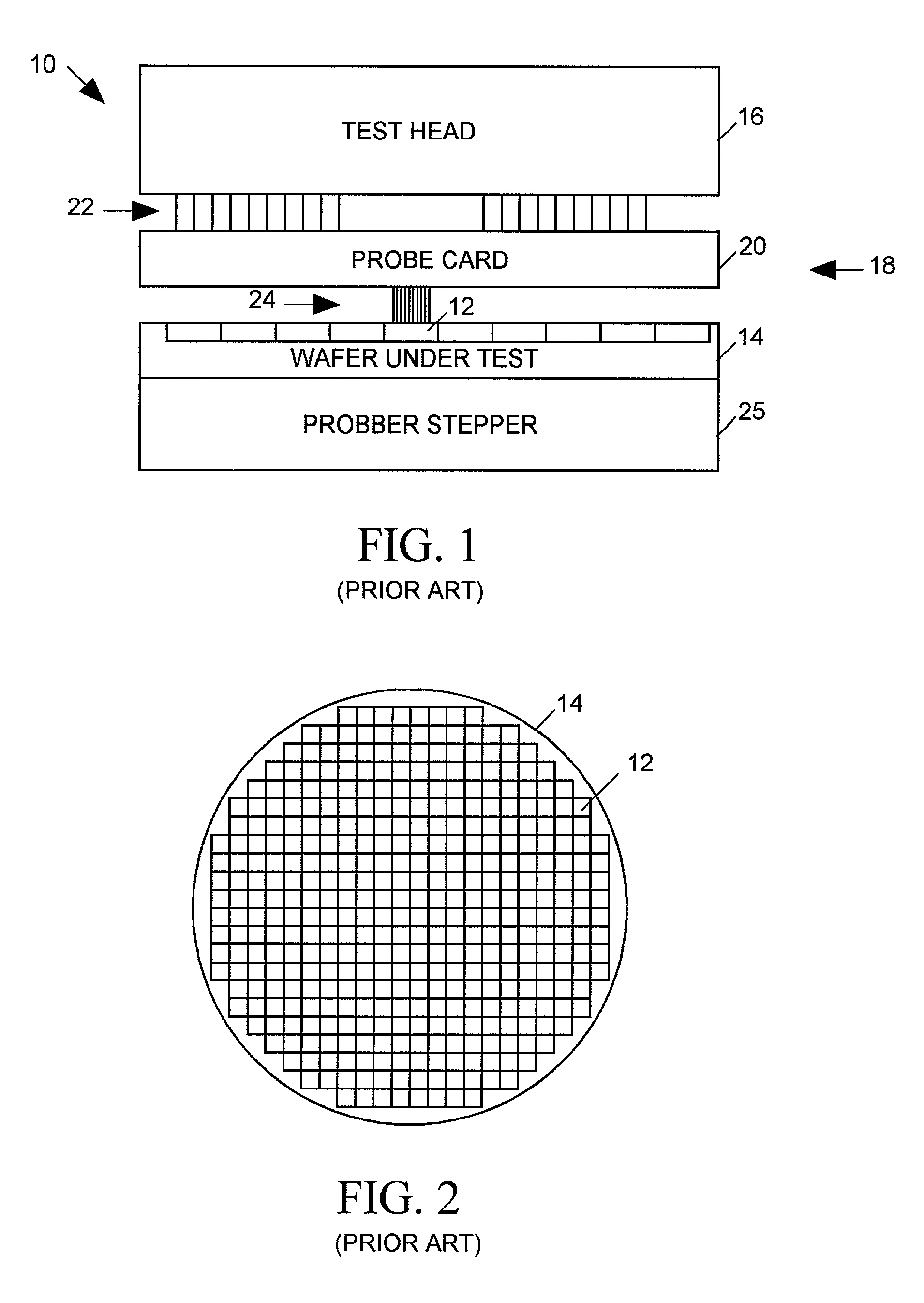
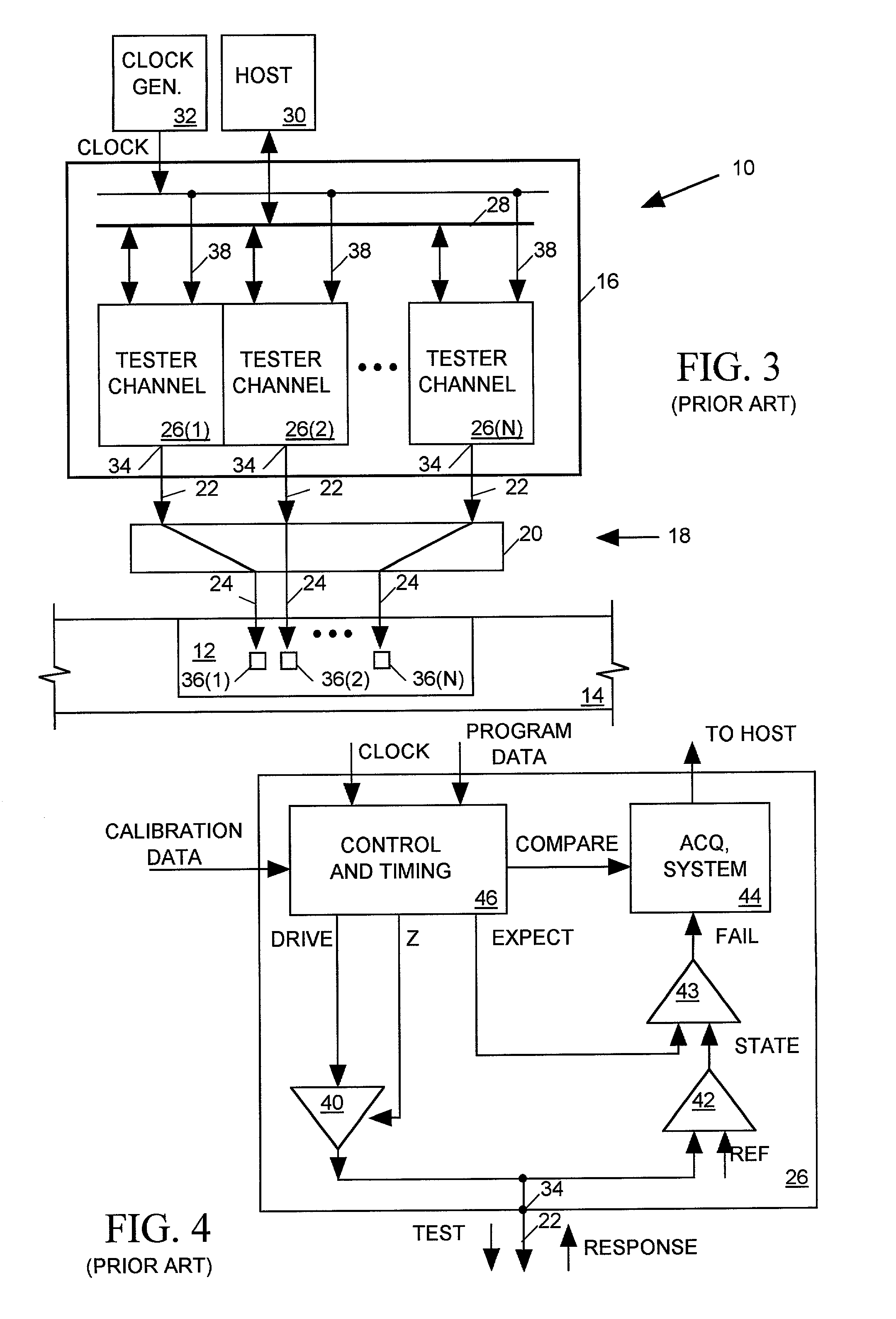
[0032] FIG. 1 is a simplified sectional elevation view of a typical prior art IC tester 10 designed to test an IC 12 while still in the form of a die on a semiconductor wafer 14. FIG. 2 is a plan view of a wafer 14 implementing a large number of ICs 12. Tester 10 includes "test head" 16, a chassis containing circuit boards implementing a set of tester channels. Each tester channel is capable of supplying a test signal input to a bond pad or other test point of IC 12 and / or of monitoring an IC output signal produced at that bond pad to determine its state. Tester 10 also includes an interconnect system 18 linking each tester channel within test head 16 to an appropriate bon...


PUM


Abstract

A timing calibration system for a wafer level integrated circuit (IC) tester is disclosed. The tester includes a set of probes for contacting pads on a surface of an IC and having a plurality of tester channels. Each channel generates a TEST signal at a tip of a corresponding probe in response to a periodic CLOCK signal with a delay adjusted by drive calibration data supplied as input to the tester channel. The TEST signal produced by each channel includes edges occurring in a timing pattern controlled by programming data provided as input to each tester channel. To calibrate test signal timing of all channels, each channel is programmed to generate a test signal having the same repetitive edge timing pattern at the tester channel's corresponding probe tip. The test signal produced at each probe tip is then cross-correlated to a periodic reference signal having the same repetitive edge timing pattern. The drive calibration data of each channel is then iteratively adjusted to determine a value which maximizes the cross-correlation between its output test signal and the reference signal. To maximize the accuracy of the timing calibration, each repetition of the test and reference signal edge pattern provides pseudo-randomly distributed time intervals between successive signal edges.

Description

[0001] The present application is a continuation-in-part of copending application Ser. No. 09 / 589,399 filed Jun. 20, 2000.[0002] 1. Field of the Invention[0003] The present invention relates in general to integrated circuit (IC) wafer testers and in particular to a system for calibrating signal timing of IC wafer tester channels to compensate for variation in signal paths between the tester and test probe points on a calibration substrate.[0004] 2. Description of Related Art[0005] Integrated circuits (ICs) are fabricated in the form of die on a semiconductor wafer but are thereafter separated and packaged. To avoid the cost of packaging defective ICs an IC tester can test ICs while they are still in wafer form. An IC tester tests an IC by sending a sequence of test signals to its input terminals and monitoring the output signals produced by the IC to determine whether they behave as expected. A typical integrated circuit tester includes a "test head" containing circuit boards implem...

Claims


Application Information

Patent Timeline
IPC IPC(8): G01R31/28G01R31/317G01R31/319H01L21/66
CPCG01R31/318385G01R31/3191G01R31/31905G01R31/00
Inventor MILLER, CHARLES A.
Owner FORMFACTOR INC
Why Eureka
Try Eureka