Method of etching semiconductor device using neutral beam and apparatus for etching the same

a technology of neutral beam and semiconductor device, which is applied in the direction of masers, electric discharge tubes, decorative arts, etc., can solve the problems of gate dielectric charge-up or polysilicon notching, electrical damage as well as physical damage, physical and electrical damage to the semiconductor substrate or the specific material layer, etc., and achieve the effect of reducing contamination

Inactive Publication Date: 2002-05-23
SUNGKYUNKWAN UNIVERSITY
View PDF2 Cites 26 Cited by
  • Summary
  • Abstract
  • Description
  • Claims
  • Application Information

AI Technical Summary

Benefits of technology

0016] Further, only ions having a predetermined direction are extracted to drastically reduce co

Problems solved by technology

The bombardment of such ions causes physical and electrical damages to the semiconductor substrate or the specific material layer.
Dangling bonds may result in electrical damage as well as physical damage.
As electrical damage, there is gate dielectric charge-up or polysilicon notching due to photoresist charging.
Besides this physical and electrical damages, there is also possible contamination by materials of a chamber or the contamination of a surface layer by a reactive gas such as the generation of C-F polymers caused by the use of a CF-based gas.
Physical and electrical damages due to the bombardment of ions reduces the reliability of nanosc

Method used


Image

  • Method of etching semiconductor device using neutral beam and apparatus for etching the same
  • Method of etching semiconductor device using neutral beam and apparatus for etching the same
  • Method of etching semiconductor device using neutral beam and apparatus for etching the same

Examples


Embodiment Construction

[0025] Hereinafter, embodiments of the present invention will be described in detail with reference to the attached drawings. However, the embodiments of the present invention may be modified into various other forms, and the scope of the present invention must not be interpreted as being restricted to the embodiments. The embodiments are provided to more completely explain the present invention to those skilled in the art.

[0026]

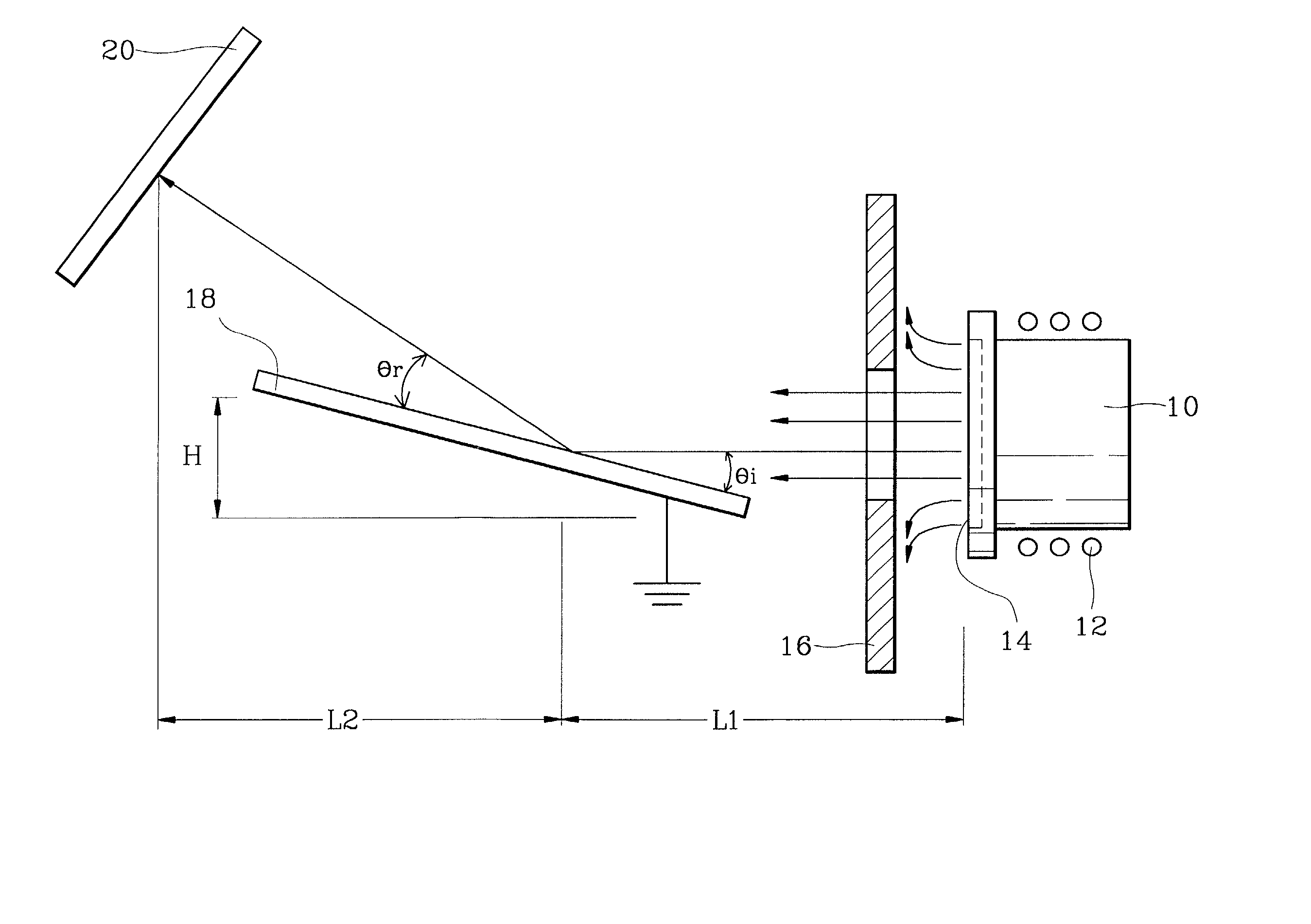
[0027] FIG. 1 is a schematic diagram of an apparatus for etching a semiconductor device according to a first embodiment of the present invention. FIG. 1 is a simplified diagram to explain the principle of the present invention, and elements shown in FIG. 1 are included in a chamber under moderate vacuum.

[0028] Describing an etching method of the present invention, an ion beam having a predetermined polarity is extracted from an ion source and then accelerated. An accelerated ion beam is reflected by a reflector and neutralized into a neutral beam. A substra...


PUM

PropertyMeasurementUnit
Angleaaaaaaaaaa
Angleaaaaaaaaaa
Polarityaaaaaaaaaa

Abstract

A method and an apparatus for etching a semiconductor device which can perform an etching process without causing electrical and physical damages using a neutral beam generated by a simple apparatus. In the method, ions of an ion beam having a predetermined polarity are extracted from an ion source and accelerated. An accelerated ion beam is reflected by a reflector and neutralized. A substrate to be etched positioned in the path of the neutral beam in order to etch a special material layer on the substrate with the neutral beam. The gradient of the reflector is adjusted to control an angle of incidence of the ion beam incident on the reflector, and a voltage is applied to the reflector to control the path of an incident ion beam.

Description

BACKGROUND OF THE INVENTION[0001] 1. Field of the Invention[0002] The present invention relates to a method of etching a semiconductor device and an apparatus for etching the same, and more particularly, to a method of etching a nanoscale semiconductor device and an apparatus for etching the same without damage by using a neutral beam.[0003] 2. Description of the Related Art[0004] As an increase in the integration density of semiconductor devices has been required, the design rule of integrated semiconductor circuits has been reduced. Thus, a critical dimension of 0.25 .mu.m or less is needed. Ion enhanced etching tools, such as a high density plasma etcher and a reactive ion etcher are mainly used as etching tools for realizing nanoscale semiconductor devices. In such case, high density ions having energies of a few hundred eV bombard a semiconductor substrate or a specific material layer on the semiconductor substrate for anisotropic etching. The bombardment of such ions causes ph...

Claims


Application Information

Patent Timeline
IPC IPC(8): C23F1/00H01L21/306H01J37/305H01J37/317H01L21/00H01L21/302H01S1/00
CPCH01J37/3053H01J37/317H01L21/67069H01L21/302H01J2237/3174H01L21/306
Inventor YEOM, GEUN-YOUNGLEE, DO-HAING
Owner SUNGKYUNKWAN UNIVERSITY
Why Eureka
Try Eureka