Semiconductor device having thin film transistor for supplying current to driven element

a technology of semiconductor devices and transistors, applied in semiconductor devices, solid-state devices, transistors, etc., can solve problems such as pixel luminance variations, and achieve the effect of avoiding problems in thin film transistors

Inactive Publication Date: 2002-06-13
SANYO ELECTRIC CO LTD
View PDF0 Cites 23 Cited by
  • Summary
  • Abstract
  • Description
  • Claims
  • Application Information

AI Technical Summary

Benefits of technology

0008] The present invention has been conceived in view of the above-described problems, and aims to provi

Problems solved by technology

However, as the laser irradiating conditions are varied and not always the same, resulting variation in crystal properties of the thin film transistors leads

Method used


Image

  • Semiconductor device having thin film transistor for supplying current to driven element
  • Semiconductor device having thin film transistor for supplying current to driven element
  • Semiconductor device having thin film transistor for supplying current to driven element

Examples


first embodiment

[0031] [First Embodiment]

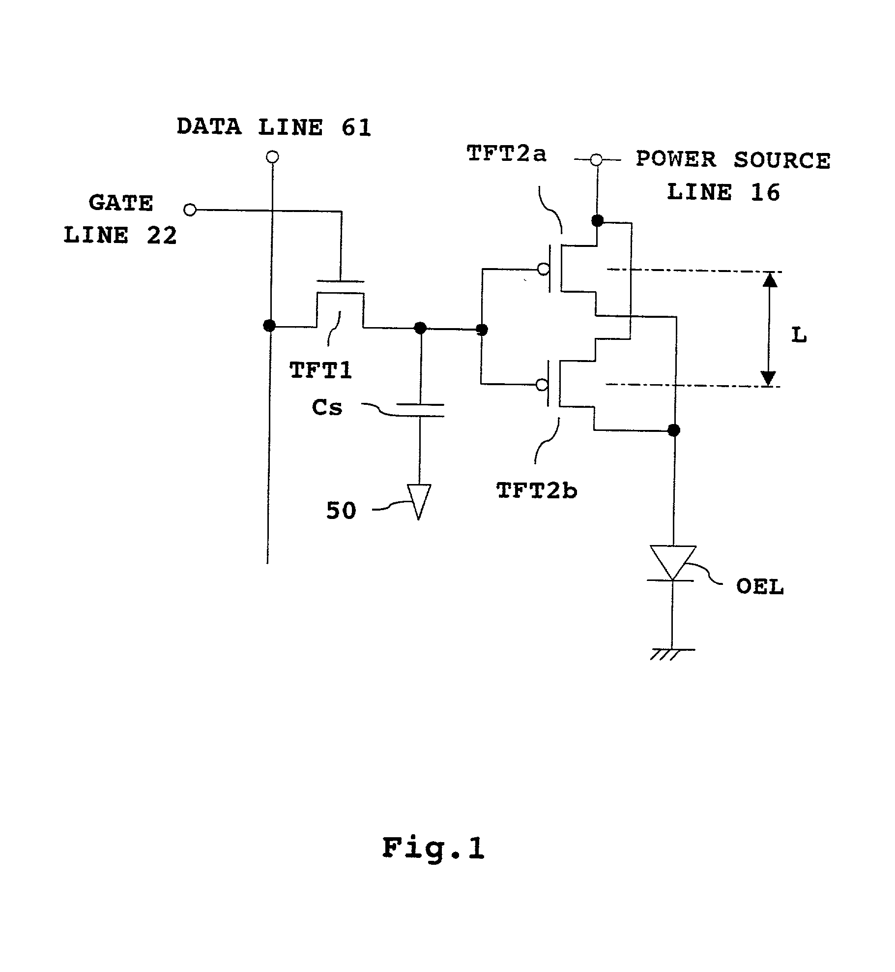
[0032] FIG. 1 shows a circuit configuration for each pixel of an organic EL display panel of an active matrix type. For a single pixel, an organic EL element OEL, a thin film transistor TFT1 for switching, TFTs for driving elements (TFT2a and TFT2b), and a storage capacitor Cs are provided. The N-channel thin film transistor TFT1 has a gate connected to a gate line (selection line) 22, a drain connected to a data line 61, and a source connected to gates of the two P-channel thin film transistors TFT2a and TFT2b connected in parallel. The thin film transistors TFT2a and TFT2b each have a source connected to a power source line 16, and a drain connected in common to the organic EL element OEL whose other end is connected to a constant potential (Vcom). The gates of the thin film transistors TFT2a and TFT2b are connected to the storage capacitor Cs whose other end is connected to a power source 50.

[0033] When a signal at a level sufficient to turn on the N-chan...

second embodiment

[0055] [Second Embodiment]

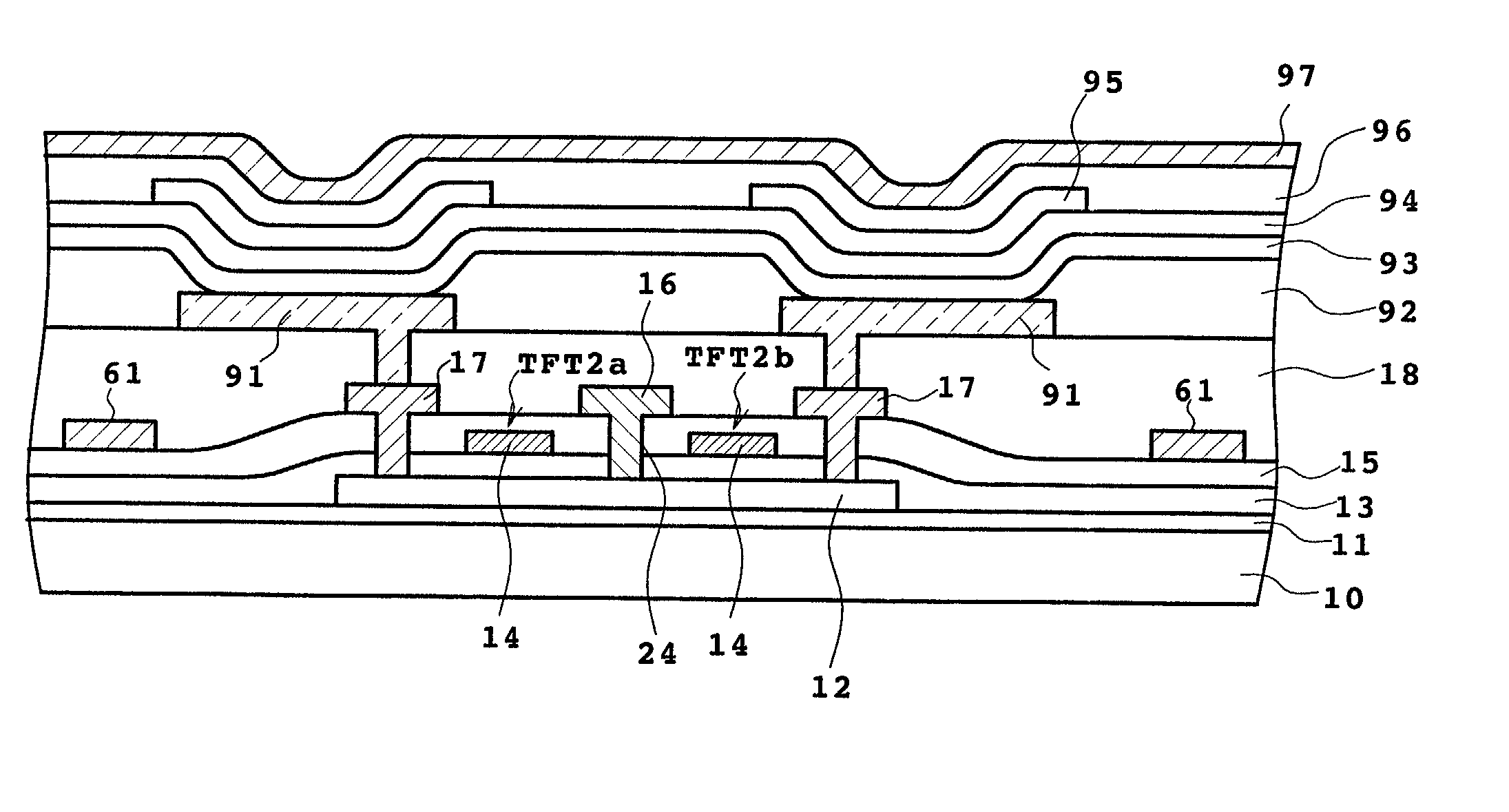
[0056] Next, another exemplary pixel configuration will be described as a second embodiment of the present invention with reference to FIG. 6. The elements corresponding to those described above are labeled with the same numerals and characters. Mainly the layouts of the transistors TFT1 and TFT2, the storage capacitor Cs, and the organic EL element 60 for each pixel differ from those in the first embodiment, and the cross sectional structures of the respective circuit elements are the same as those described above and as shown in FIG. 5.

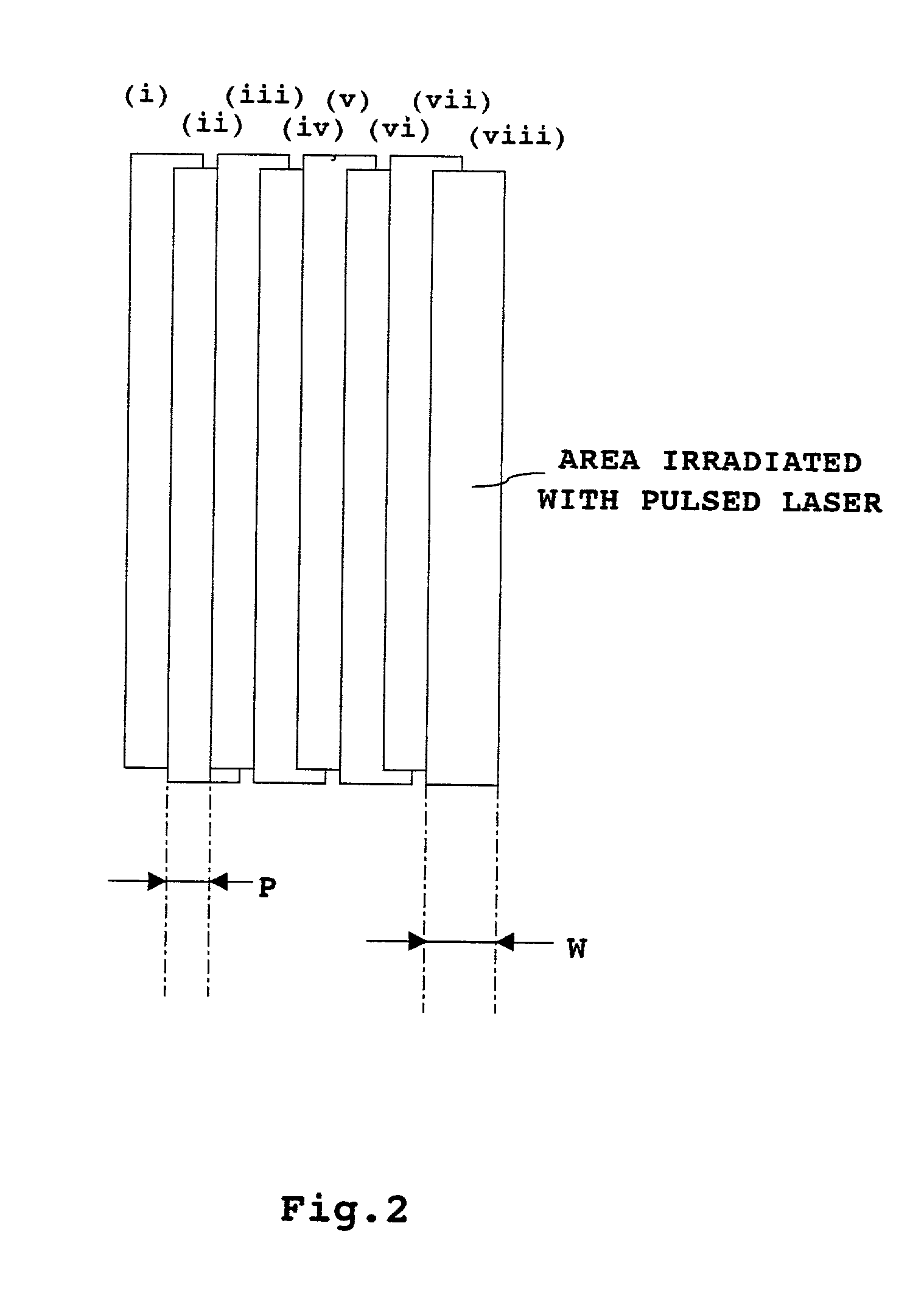
[0057] In the example of FIG. 6, the laser used for annealing is set to scan in the column direction of the figure (the direction in which the data line 61 extends), and the thin film transistor TFT2 supplying an electric current from the power source line 16 to the organic EL element 60 for driving is disposed such that the channel (12c) length direction runs substantially parallel to the scanning direction of the annealin...


PUM


Abstract

Thin film transistors TFT2a and TFT2b for driving elements are formed in parallel between a power source line (16) and an organic EL element (60), and active layers (12) of the transistors TFT2a and TFT2b are spaced apart in a scanning direction of a laser used for annealing for polycrystallization. As a result, the annealing conditions for the transistors TFT2a and TFT2b will not be exactly the same, thereby reducing the chance of a same problem being caused in both transistors TFT2a and TFT2b.

Description

[0001] 1. Field of the Invention[0002] The present invention relates to a semiconductor device having a plurality of thin film transistors on a substrate that use a semiconductor layer annealed with a pulsed laser as a channel region, and more particularly to a technique for overcoming variation in characteristics of the thin film transistors.[0003] 2. Description of the Related Art[0004] Organic electroluminescence (hereinafter referred to as "EL") display panels using organic EL elements have been known as flat panel displays. While liquid crystal displays (LCDs) are widely used as flat panel displays, LCDs merely transmit or reflect light from a light source separately provided, and are not self-emissive. On the other hand, organic EL display elements are used in a self-emissive display for supplying a current to an organic EL layer provided between an anode and a cathode to cause the layer to emit light, and therefore back lighting is not required, as opposed to the LCDs. Organi...

Claims


Application Information

Patent Timeline
IPC IPC(8): H01L21/20H01L21/324H01L21/336H01L29/786H01L51/50
CPCH01L21/2026H01L21/02686H01L21/02488H01L21/02678H01L21/02532H01L21/02691H01L21/02587H01L21/324
Inventor YAMADA, TSUTOMUANZAT, KATSUYA
Owner SANYO ELECTRIC CO LTD
Why Eureka
Try Eureka