Photodetector utilizing a HEMTstructure

a photodetector and hemt structure technology, applied in the direction of basic electric elements, electrical apparatus, semiconductor devices, etc., can solve the problems of difficult modification of hole mobility, limiting the current impulse response of the hole, and limiting the speed performance of the msm photodetector

Inactive Publication Date: 2002-06-13
GWANGJU INST OF SCI & TECH
View PDF0 Cites 27 Cited by
  • Summary
  • Abstract
  • Description
  • Claims
  • Application Information

AI Technical Summary

Problems solved by technology

Therefore, the hole current impulse response is a limiting factor in determining the speed performance of the MSM ...

Method used


Image

  • Photodetector utilizing a HEMTstructure
  • Photodetector utilizing a HEMTstructure
  • Photodetector utilizing a HEMTstructure

Examples


first embodiment

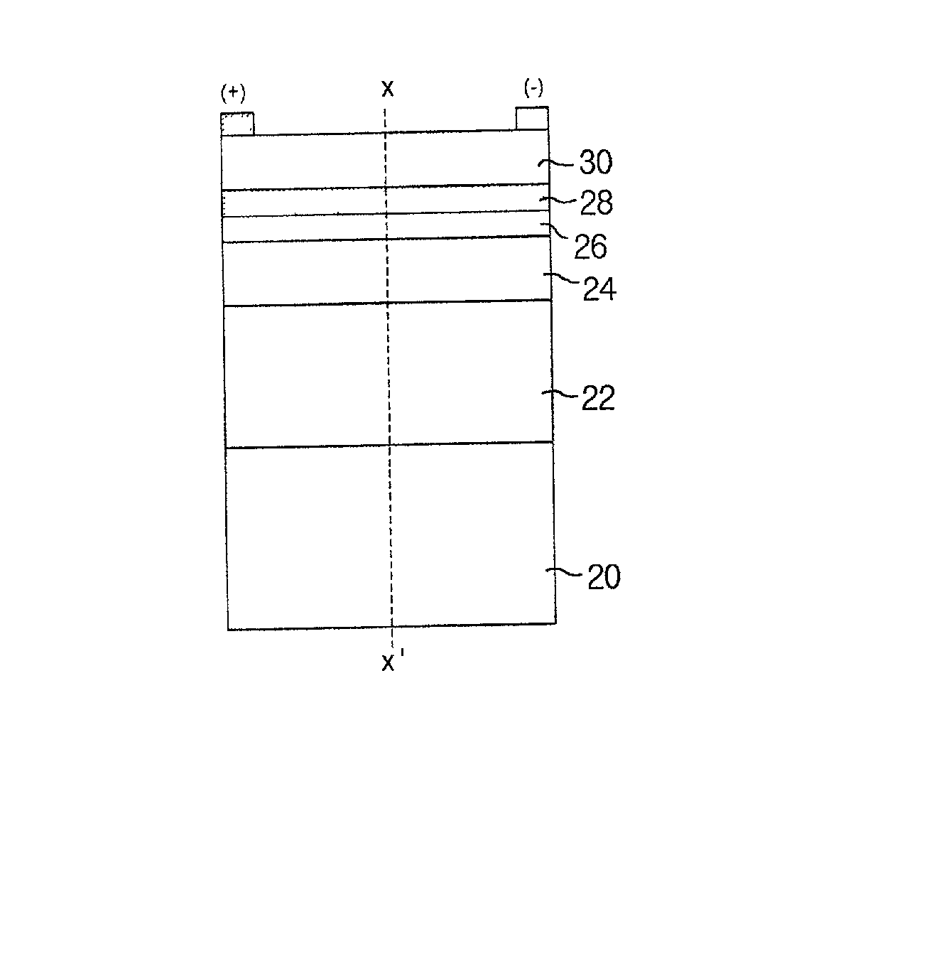
[0038] The following describes the epitaxial layer structure of the MSM photodetector according to the present invention with reference to FIG. 4.

[0039] The buffer layer 20 is an undoped epitaxial layer grown on the semi-insulating substrate in order to improve the quality of the epitaxial layer.

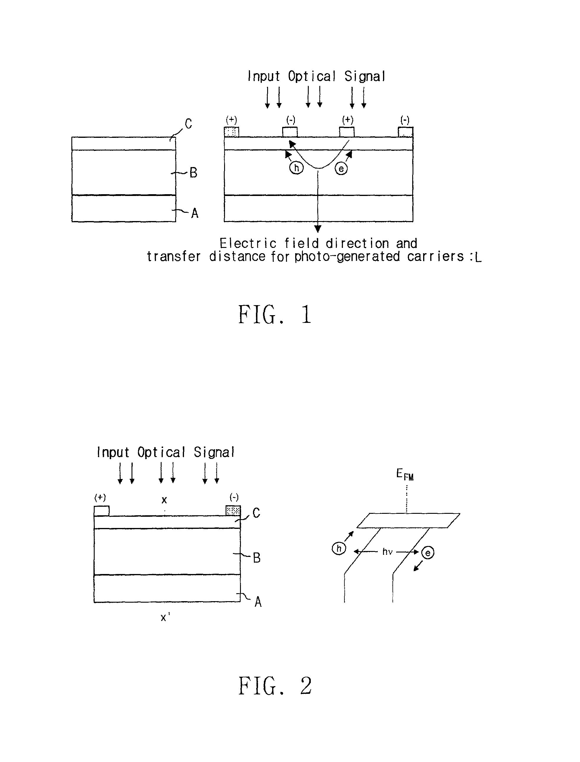
[0040] The channel layer 22, grown on the buffer layer 20, is a p-doped epitaxial layer used as an absorption layer of the MSM photodetector, in which electron hole pairs are generated by absorbing the optical signal and transported by electric field.

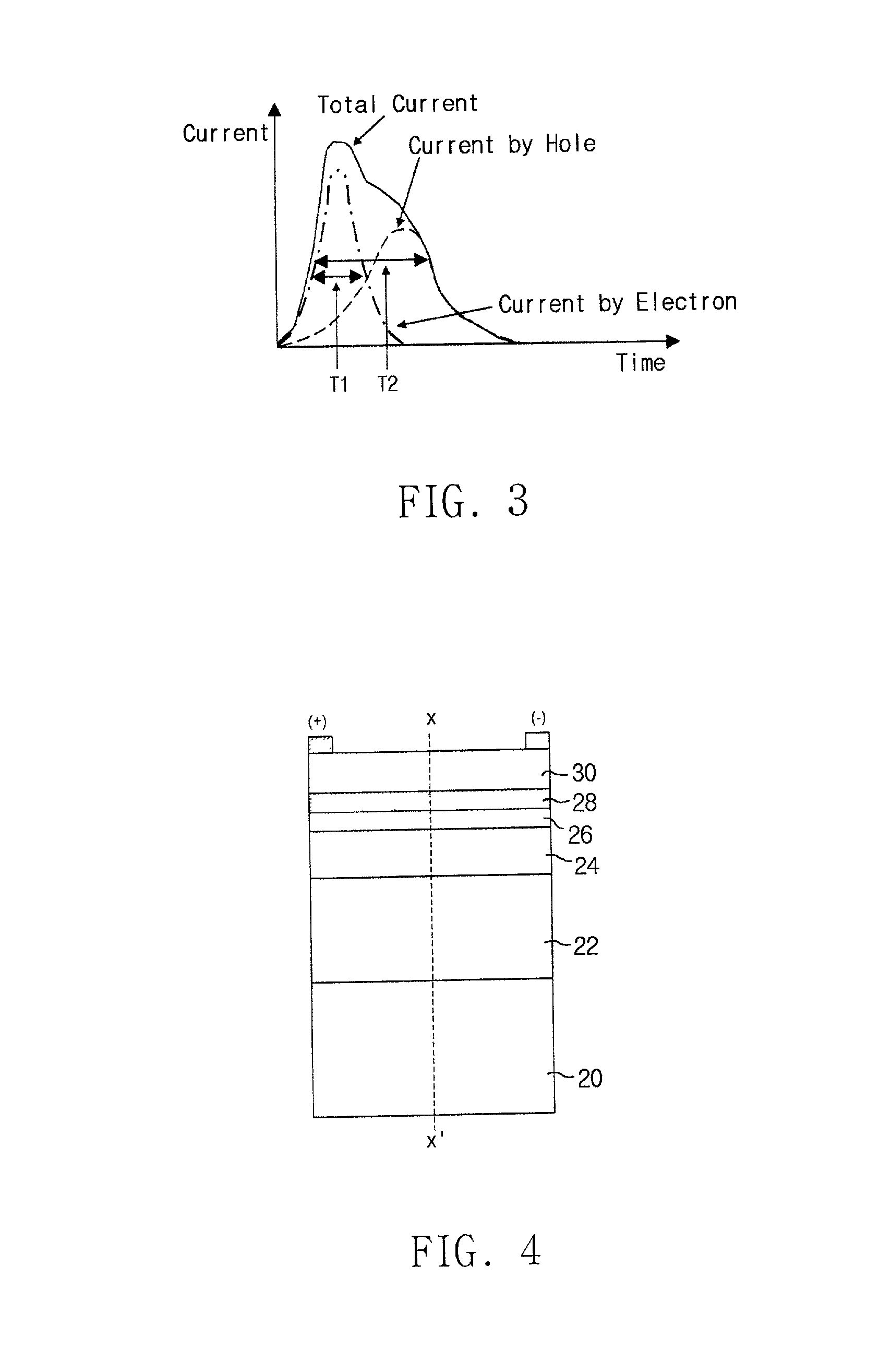
[0041] The thickness and doping concentration of the p-doped layer 22 have to be optimized so that the layer can be completely depleted at the operating bias voltage of the MSM photodetector. When the p-doped epitaxial layer 22 is fully depleted, it generates an electric field that moves the photo-generated electrons toward the metal electrodes and the photo-generated holes away from the metal electrodes as shown in FIG. 6.

[0042] The other chann...

second embodiment

[0055] So far MSM photodetector structures based upon the delta-doped HEMT structure are described. The following describes MSM photodetector structures based upon the uniform-doped HEMT structure according to the present invention with reference to FIG. 8.

[0056] The first one is a GaAs-based photodetector structure. The structure comprises; an undoped Al.sub.xGa.sub.1-xAs (0.ltoreq..times..ltoreq.0.4) buffer layer 20 grown on a semi-insulating GaAs substrate, a p-type ln.sub.xGa.sub.1-xAs (0.ltoreq..times..ltoreq.0.-25) channel layer 22 grown on the Al.sub.xGa.sub.1-xAs (0.ltoreq..times..ltoreq.0.4) buffer layer 20, an undoped ln.sub.xGa.sub.1-xAs (0.ltoreq..times..ltoreq.0.25) channel layer 24 grown on the p-type ln.sub.xGa.sub.1-xAs (0.ltoreq..times..ltoreq.0.25) channel layer 22, an undoped barrier layer 26 which is formed by either Al.sub.xGa.sub.1-xAs (0.ltoreq..times..ltoreq.0.4) or ln.sub.xGa.sub.1-xP (0.45.ltoreq..times..ltoreq.0.55) grown on the ln.sub.xGa.sub.1-xAs (0.lto...


PUM


Abstract

The present invention relates to MSM photodetectors based on the high electron mobility transistor (HEMT) structure. More specifically, the present invention relates to MSM photodetectors based on the high electron mobility transistor (HEMT) structure that use a barrier layer of the HEMT structure as a Schottky barrier layer of the photodetector and use the channel layer of the HEMT structure as an absorption layer of the photodetector by doping the bottom part of the channel layer with a p-type dopant. Modification of the HEMT structure for the MSM photodetector can enhance electron current and suppress hole current, resulting in an impulse photocurrent response having a narrow pulse width. The present invention comprises an undoped buffer layer grown on the semi-insulating substrate, a p-doped channel layer that is used as an absorption layer grown on the said buffer layer, an undoped channel layer that is used as an absorption layer grown on the said channel layer, an undoped barrier layer that is composed of a material having a larger band gap energy than the said channel layers grown on the said undoped channel layer, a heavily n-type delta-doped barrier layer that is composed of a material having a larger band gap energy than the said channel layers grown on the said undoped barrier layer, and an undoped barrier layer that is composed of a material having a larger band gap energy than the said channel layers grown on the said heavily n-type delta-doped barrier layer.

Description

[0001] 1. Field of the Invention[0002] The present invention relates to metal-semiconductor-metal (MSM) photodetectors utilizing a high electron mobility transistor (HEMT) structure. More specifically, the present invention relates to MSM photodetectors utilizing the HEMT structure, wherein the barrier layer of the HEMT is used as a Schottky barrier layer of the MSM photodetector and the channel layer of the HEMT is used as an absorption layer of the MSM photodetector. While utilizing the basic structure of the HEMT for the MSM photodetector, the channel layer of the HEMT structure is modified to improve the speed performance of the MSM photodetector. The channel layer of the HEMT structure used for a transistor is generally undoped. On the contrary, the bottom part of the channel layer of the HEMT structure used for the MSM photodetector is doped with a p-type dopant. By utilizing the HEMT structure having the modified channel layer for the MSM photodetector, the speed performance ...

Claims


Application Information

Patent Timeline
IPC IPC(8): H01L29/778H01L31/0328H01L31/0336H01L31/072H01L31/109
CPCH01L31/1085H01L31/101H01L29/778
Inventor SONG, JONG IN
Owner GWANGJU INST OF SCI & TECH
Why Eureka
Try Eureka